5
LTC1517-3.3
APPLICATIONS INFORMATION
WUU
U
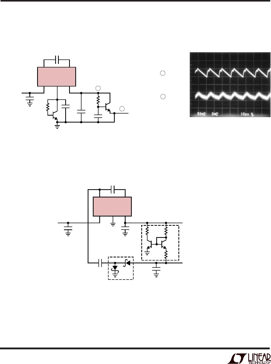
Output Ripple
Normal LTC1517-3.3 operation produces voltage ripple
on the V
OUT
pin. Output voltage ripple is required for the
parts to regulate. Low frequency ripple exists due to the
hysteresis in the sense comparator and propagation de-
lays in the charge pump enable/disable circuits. High
frequency ripple is also present mainly from the ESR
(equivalent series resistance) in the output capacitor.
Typical output ripple with V
IN
= 2.5V under maximum load
is 75mV peak-to-peak with a low ESR 3.3µF output capaci-
tor (minimum recommended C
OUT
). For applications
requiring V
IN
to exceed 3.3V or for applications requiring
less than 75mV of peak-to-peak ripple, a 6.8µF to 10µF
C
OUT
capacitor is recommended. Slight further decreases
in output ripple can be achieved by using C
OUT
capacitors
larger than 10µF.
Short-Circuit/Thermal Protection
During short-circuit conditions, the LTC1517-3.3 will draw
between 20mA and 150mA from V
IN
, causing a rise in
junction temperature. On-chip thermal shutdown circuitry
disables the charge pump once the junction temperature
exceeds approximately 160°C. The charge pump is
reenabled once the junction temperature drops to approxi-
mately 145°C. The LTC1517-3.3 will cycle in and out of
thermal shutdown indefinitely without latchup or damage
until the V
OUT
short is removed.
Operation
The LTC1517-3.3 uses a switched-capacitor charge pump
to boost V
IN
to a 3.3V ±4% regulated output. The part
achieves regulation by sensing the output voltage through
an internal resistor divider and enabling the charge pump
when the divided output droops below the comparator’s
lower trip point (set by V
REF
). When the charge pump is
enabled, a 2-phase nonoverlapping clock controls the
internal charge pump switches. Flying capacitor C1 is
charged to V
IN
on phase one of the clock. On phase two of
the clock, C1 is stacked in series with V
IN
and connected
to V
OUT
through an internal switch. This sequence of
charging and discharging the flying capacitor occurs at a
free running frequency of 700kHz (typ) and continues until
the divided output voltage reaches the upper trip point of
the comparator. Once the output is back in regulation, the
charge pump is disabled. This method of bursting the
charge pump on and off enables the LTC1517-3.3 to
achieve high efficiency at extremely low output loads.
Capacitor Selection
For best performance, it is recommended that low ESR
capacitors be used for both C
IN
and C
OUT
to reduce noise
and ripple. The C
IN
and C
OUT
capacitors should be either
ceramic or tantalum and should be 3.3µF or greater.
Ceramic capacitors will provide the smallest size for a
given capacitance. If the input source impedance is very
low (< 0.5Ω), C
IN
may not be needed. Ceramic capacitors
are recommended for the flying capacitor C1 with values
of 0.1µF or 0.22µF. Smaller value flying capacitors may be
used in low I
OUT
applications.