MMBD2004S-7-F

MMBD2004S
Document number: DS30281 Rev. 12 - 2
1 of 4
www.diodes.com
August 2012
© Diodes Incorporated
MMBD2004S
HIGH VOLTAGE SURFACE MOUNT DUAL SWITCHING DIODE
Features
Fast Switching Speed: Maximum of 50ns
High Reverse Breakdown Voltage: 300V
Low Leakage Current: Maximum of 100nA when V
R
= 240V at
Room Temperature
Surface Mount Package Ideally Suited for Automated Insertion
Dual Series Configuration
Totally Lead-Free & Fully RoHS Compliant (Notes 1 & 2)
Halogen and Antimony Free. “Green” Device (Note 3)
Qualified to AEC-Q101 Standards for High Reliability
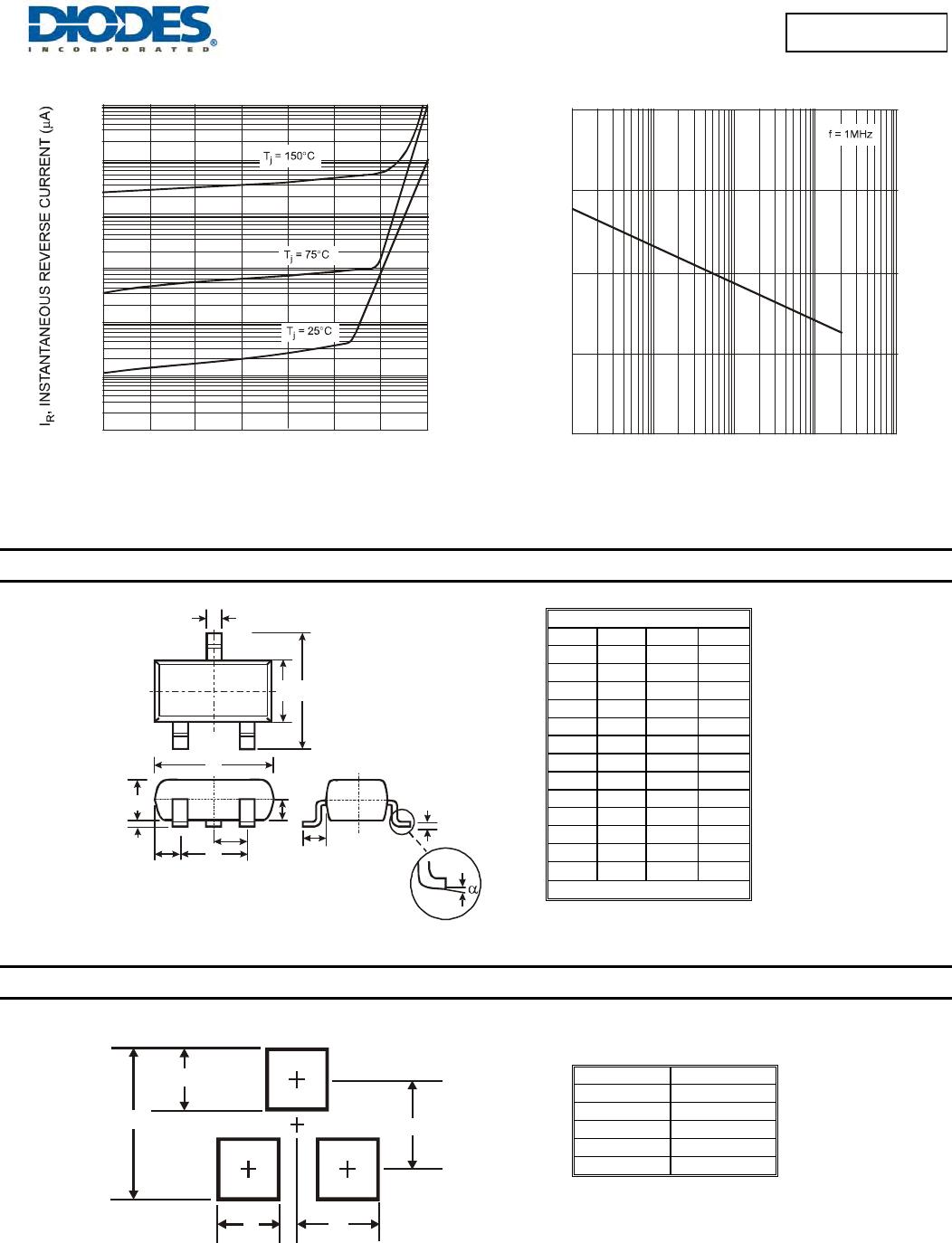
Mechanical Data
Case: SOT23
Case Material: Molded Plastic, “Green” Molding Compound. UL
Flammability Classification Rating 94V-0
Moisture Sensitivity: Level 1 per J-STD-020D
Terminals: Solderable per MIL-STD-202, Method 208
Lead Free Plating (Matte Tin Finish annealed over Alloy 42
leadframe).
Polarity: See Diagram
Weight: 0.008 grams (approximate)
Ordering Information (Note 4)
Part Number Qualification Case Packaging
MMBD2004S-7-F Commercial SOT23 3000/Tape & Reel
MMBD2004SQ-7-F Automotive SOT23 3000/Tape & Reel
Notes: 1. No purposely added lead. Fully EU Directive 2002/95/EC (RoHS) & 2011/65/EU (RoHS 2) compliant.
2. See http://www.diodes.com for more information about Diodes Incorporated’s definitions of Halogen- and Antimony-free, "Green" and Lead-free.
3. Halogen- and Antimony-free "Green” products are defined as those which contain <900ppm bromine, <900ppm chlorine (<1500ppm total Br + Cl) and
<1000ppm antimony compounds.
4. For packaging details, go to our website at http://www.diodes.com/datasheets/ap02007.pdf.
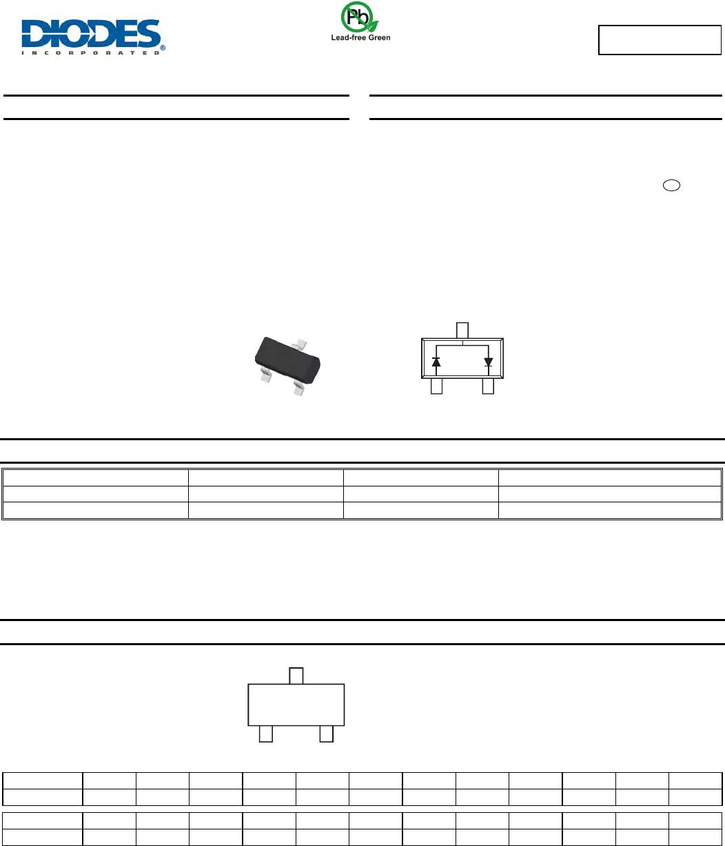
Marking Information
Date Code Key
Year 2001 2002 2003 ….. 2012 2013 2014 2015 2016 2017 2018 2019
Code M N P ….. Z A B C D E F G
Month Jan Feb Mar Apr May Jun Jul Aug Sep Oct Nov Dec
Code 1 2 3 4 5 6 7 8 9 O N D
e3
SOT23
Internal Schematic
To
p
View
Kxx = Product Type Marking Code (KA9 or KAE)
YM = Date Code Marking
Y = Year ex: Z = 2012
M = Month ex: 9 = September
KXX
YM
MMBD2004S
Document number: DS30281 Rev. 12 - 2
2 of 4
www.diodes.com
August 2012
© Diodes Incorporated
MMBD2004S
Maximum Ratings (@T
A
= +25°C, unless otherwise specified.)
Characteristic Symbol Value Unit
Repetitive Peak Reverse Voltage
V
RRM
300 V
Working Peak Reverse Voltage
DC Blocking Voltage
V
RWM
V
R
240 V
RMS Reverse Voltage
V
R
(
RMS
)
170 V
Forward Continuous Current (Note 5)
I
FM
225 mA
Peak Repetitive Forward Current (Note 5)
I
FRM
625 mA
Non-Repetitive Peak Forward Surge Current @ t = 1.0µs
@ t = 1.0s
I
FSM
4.0
1.0
A
Thermal Characteristics
Characteristic Symbol Value Unit
Power Dissipation (Note 5)
P
D
350 mW
Thermal Resistance Junction to Ambient Air (Note 5)
R
θ
JA
357
°C/W
Operating and Storage Temperature Range
T
J
, T
STG
-65 to +150
°C
Electrical Characteristics (@T
A
= +25°C, unless otherwise specified.)
Characteristic Symbol Min Max Unit Test Condition
Reverse Breakdown Voltage (Note 6)
V
(
BR
)
R
300
V
I
R
= 100µA
Forward Voltage
V
F
0.87
1.0
V
I
F
= 20mA
I
F
= 100mA
Reverse Current (Note 6)
I
R
100
nA
µA
V
R
= 240V
V
R
= 240V, T
J
= +150°C
Total Capacitance
C
T
5.0 pF
V
R
= 0, f = 1.0MHz
Reverse Recovery Time
t
rr
50 ns
I
F
= I
R
= 30mA,
I
rr
= 3.0mA, R
L
= 100Ω
Notes: 5. Part mounted on FR-4 board with recommended pad layout, which can be found on our website at http://www.diodes.com/datasheets/ap02001.pdf.
6. Short duration pulse test used to minimize self-heating effect.
0
120
8040
160
200
T , AMBIENT TEMPERATURE (ºC)
Figure 1 Power Derating Curve, Total Package
A
P
,
P
O
WE
R
DISSI
P
A
T
I
O
N (mW)
D
0
100
200
300
400
500
0
400 800 1,200
1,600 2,000
I, I
N
S
T
A
N
T
A
N
E
O
U
S
F
O
R
WA
R
D
C
U
R
R
E
N
T
(A)
F
m
V , INSTANTANEOUS FORWARD VOLTAGE (mV)
Figure 2 Typical Forward Characteristics, Per Element
F
100
1.0
10
0.1
0.01
1,000
MMBD2004S
Document number: DS30281 Rev. 12 - 2
3 of 4
www.diodes.com
August 2012
© Diodes Incorporated
MMBD2004S
0
50
100 150
200 250
300 350
V , INSTANTANEOUS REVERSE VOLTAGE (V)
Figure 3 Typical Reverse Characteristics, Per Element
R
100
1.0
10
0.1
0.01
0.001
1,000
0.7
0.8
0.01
0.1
1.0
10
100
C
,
T
O
T
AL
C
A
P
A
C
I
T
AN
C
E (p
F
)
T
Figure 4 Total Capacitance vs. Reverse Voltage
Per Element
V , DC REVERSE VOLTAGE (V)
R
0.9
1.0
1.1
Package Outline Dimensions
Suggested Pad Layout
SOT23
Dim Min Max Typ
A 0.37 0.51 0.40
B 1.20 1.40 1.30
C 2.30 2.50 2.40
D 0.89 1.03 0.915
F 0.45 0.60 0.535
G 1.78 2.05 1.83
H 2.80 3.00 2.90
J 0.013 0.10 0.05
K 0.903 1.10 1.00
K1 - - 0.400
L 0.45 0.61 0.55
M 0.085 0.18 0.11
α
0° 8° -
All Dimensions in mm
Dimensions Value (in mm)
Z 2.9
X 0.8
Y 0.9
C
2.0
E
1.35
A
M
J
L
D
F
B
C
H
K
G
K1
X
E
Y
C
Z

MMBD2004S-7-F

Mfr. #:
Manufacturer:
Diodes Incorporated
Description:
Diodes - General Purpose, Power, Switching 240V 350mW
Lifecycle:
New from this manufacturer.
Delivery:
DHL FedEx Ups TNT EMS
Payment:
T/T Paypal Visa MoneyGram Western Union

Products related to this Datasheet