MZP4729A Series
http://onsemi.com
3
ELECTRICAL CHARACTERISTICS (T
A
= 25°C unless otherwise noted, V
F
= 1.5 V Max @ I
F
= 200 mA for all types)
Device
(Note 1)
Device
Marking
Zener Voltage (Note 2) Zener Impedance (Note 3) Leakage Current
I
R
(Note 4)
V
Z
(Volts) @ I
ZT
Z
ZT
@ I
ZT
Z
ZK
@ I
ZK
I
R
@ V
R
Min Nom Max mA
W W
mA μA Max Volts mA
MZP4729A MZP4729A 3.42 3.6 3.78 69 10 400 1 100 1 1260
MZP4734A MZP4734A 5.32 5.6 5.88 45 5 600 1 10 2 810
MZP4735A MZP4735A 5.89 6.2 6.51 41 2 700 1 10 3 730
MZP4736A MZP4736A 6.46 6.8 7.14 37 3.5 700 1 10 4 660
MZP4737A MZP4737A 7.13 7.5 7.88 34 4 700 0.5 10 5 605
MZP4738A MZP4738A 7.79 8.2 8.61 31 4.5 700 0.5 10 6 550
MZP4740A MZP4740A 9.50 10 10.50 25 7 700 0.25 10 7.6 454
MZP4741A MZP4741A 10.45 11 11.55 23 8 700 0.25 5 8.4 414
MZP4744A MZP4744A 14.25 15 15.75 17 14 700 0.25 5 11.4 304
MZP4745A MZP4745A 15.20 16 16.80 15.5 16 700 0.25 5 12.2 285
MZP4746A MZP4746A 17.10 18 18.90 14 20 750 0.25 5 13.7 250
MZP4749A MZP4749A 22.80 24 25.20 10.5 25 750 0.25 5 18.2 190
MZP4750A MZP4750A 25.65 27 28.35 9.5 35 750 0.25 5 20.6 170
MZP4751A MZP4751A 28.50 30 31.50 8.5 40 1000 0.25 5 22.8 150
MZP4752A MZP4752A 31.35 33 34.65 7.5 45 1000 0.25 5 25.1 135
MZP4753A MZP4753A 34.20 36 37.80 7.0 50 1000 0.25 5 27.4 125
1. TOLERANCE AND TYPE NUMBER DESIGNATION
The type numbers listed have a standard tolerance on the nominal zener voltage of ±5%.
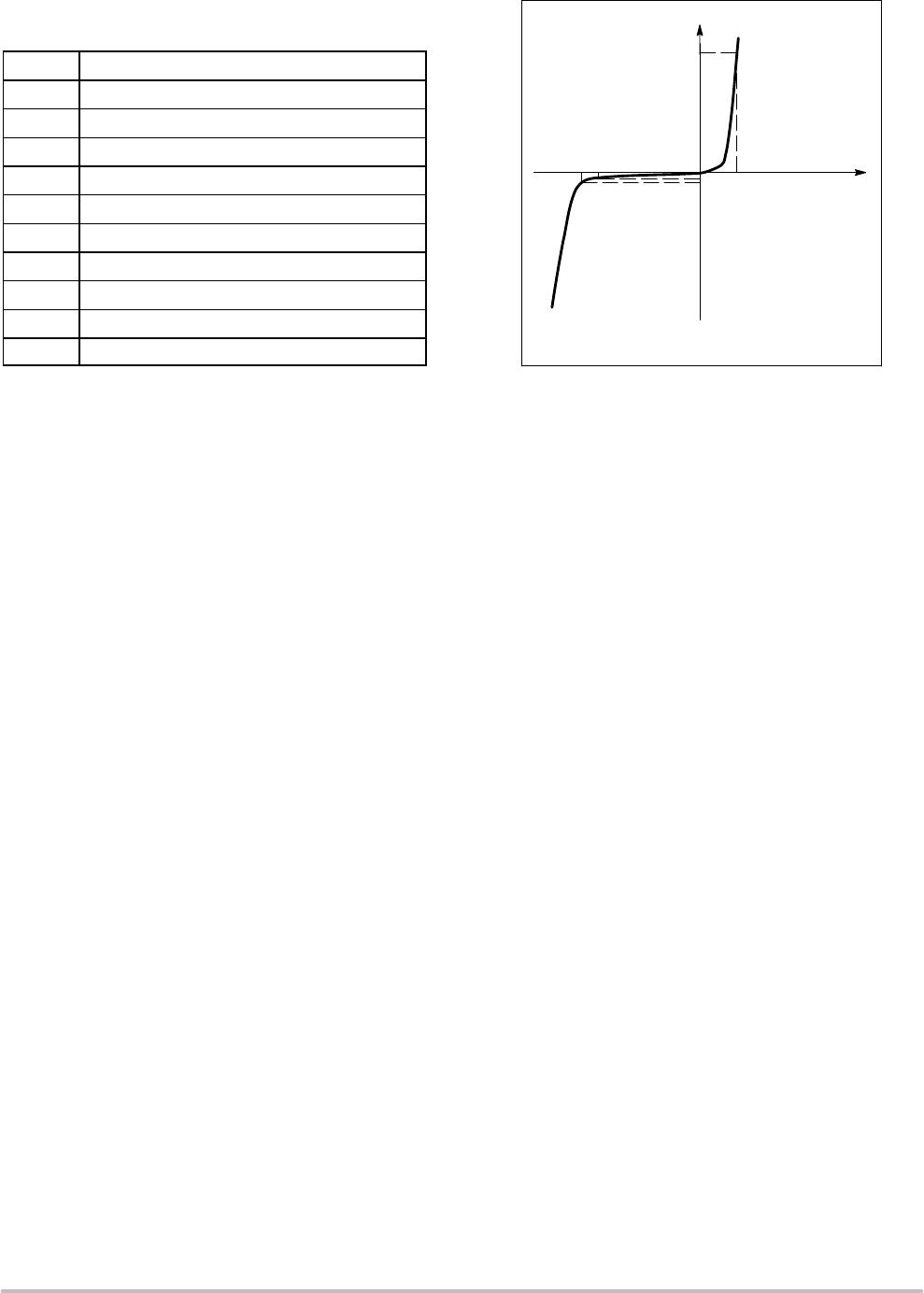
2. ZENER VOLTAGE (V
Z
) MEASUREMENT
ON Semiconductor guarantees the zener voltage when measured at 90 seconds while maintaining the lead temperature (T
L
) at 30°C ±1°C,
3/8″ from the diode body.
3. ZENER IMPEDANCE (Z
Z
) DERIVATION
The zener impedance is derived from 60 seconds AC voltage, which results when an AC current having an rms value equal to 10% of the
DC zener current (I
ZT
or I
ZK
) is superimposed on I
ZT
or I
ZK
.
4. SURGE CURRENT (I
R
) NON−REPETITIVE
The rating listed in the electrical characteristics table is maximum peak, non−repetitive, reverse surge current of 1/2 square wave or
equivalent sine wave pulse of 1/120 second duration superimposed on the test current, I
ZT
, per JEDEC standards. However, actual device
capability is as described in Figure 3 of the General Data sheet for Surmetic 30s.
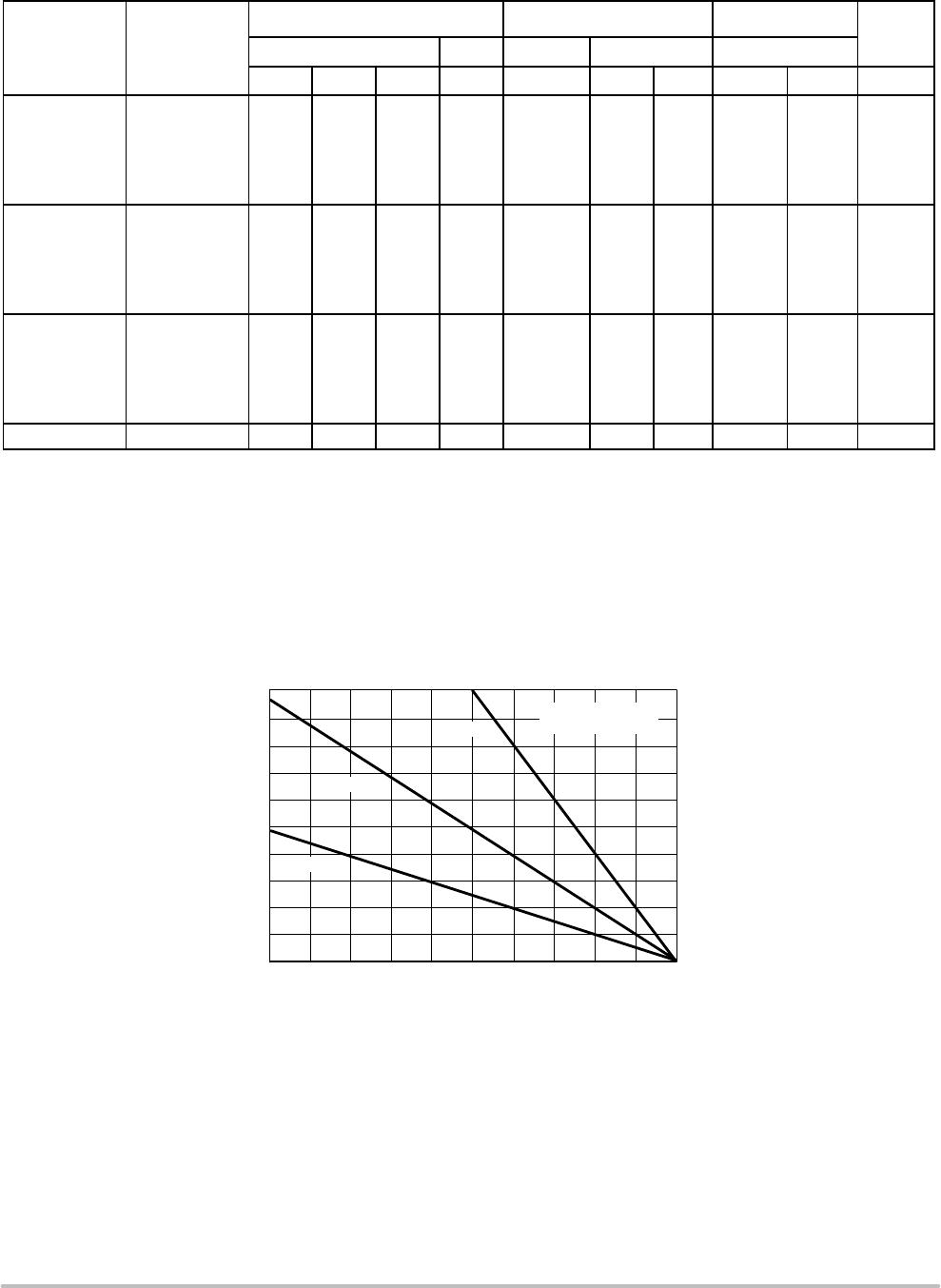
Figure 1. Power Temperature Derating Curve
T
L
, LEAD TEMPERATURE (°C)
0 20 40 60 20080 100 120 140 160 180
0
1
2
3
4
5
L = 1/8″
L = 3/8″
L = 1″
L = LEAD LENGTH
TO HEAT SINK
P
D
, MAXIMUM STEADY STATE
POWER DISSIPATION (WATTS)