MAX5432–MAX5435
32-Tap, Nonvolatile, I
2
C, Linear, Digital
Potentiometers
8 _______________________________________________________________________________________
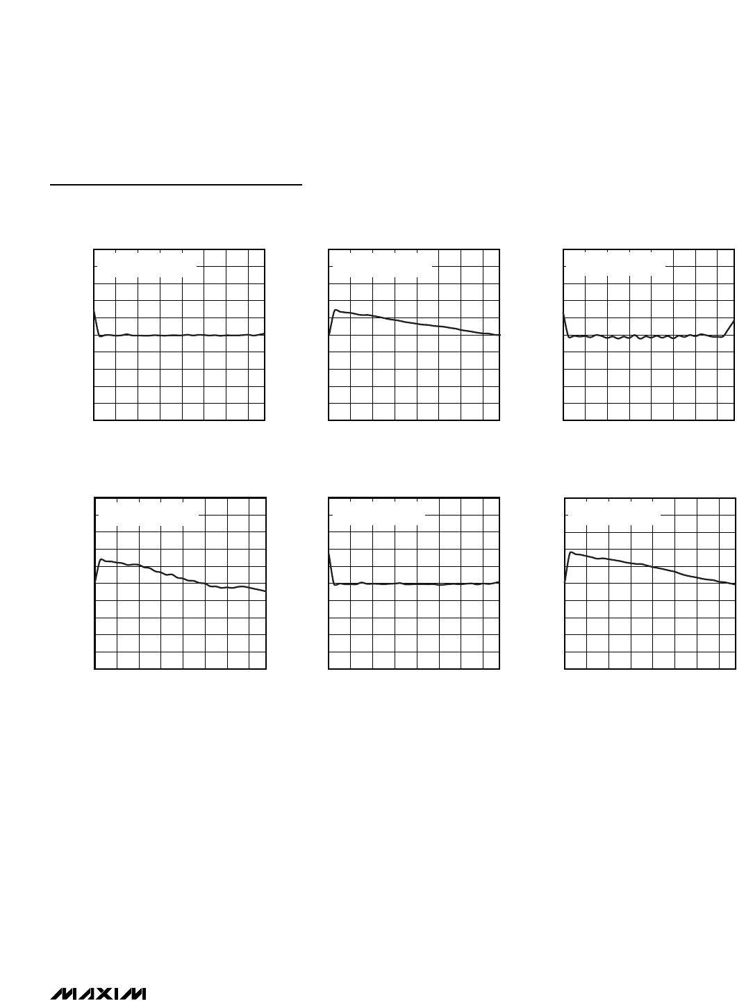
Detailed Description
The MAX5432–MAX5435 contain a resistor array with
31 resistive elements. The MAX5432/MAX5434 provide
a total end-to-end resistance of 50kΩ, and the
MAX5433/MAX5435 provide an end-to-end resistance
of 100kΩ.
The MAX5432/MAX5433 allow access to the high, low,
and wiper terminals for a standard voltage-divider con-
figuration. Connect H, L, and W in any desired configu-
ration as long as their voltages fall between GND and
V
DD
. The MAX5434/MAX5435 are variable resistors
with H internally connected to the wiper.
A simple 2-wire I
2
C-compatible serial interface moves
the wiper among the 32 tap points. Eight data bits, an
address byte, and a control byte program the wiper
position. A nonvolatile memory stores and recalls the
wiper position in the nonvolatile memory upon power-up.
The nonvolatile memory is guaranteed for 200,000 wiper
store cycles and 50 years for wiper data retention.
Digital Interface
The MAX5432–MAX5435 feature an internal, nonvolatile
EEPROM that returns the wiper to its previously stored
position at power-up. The shift register decodes the
control and address bits, routing the data to the proper
memory registers. Write data to the volatile memory
register to immediately update the wiper position, or
write data to the nonvolatile register for storage. Writing
to the nonvolatile register takes a minimum of 12ms.
The volatile register retains data as long as the device
is enabled and powered. Removing power clears the
volatile register. The nonvolatile register retains data
even after power is removed. Upon power-up, the
power-on reset circuitry and internal oscillator control
the transfer of data from the nonvolatile register to the
volatile register.
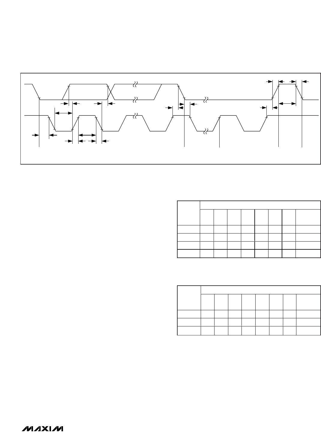
Serial Addressing
The MAX5432–MAX5435 operate as a slave that sends
and receives data through an I
2
C- and SMBus™-com-
patible 2-wire interface. The interface uses a serial data
access (SDA) line and a serial clock line (SCL) to
achieve bidirectional communication between
master(s) and slave(s). A master, typically a microcon-
troller, initiates all data transfers to and from the
MAX5432–MAX5435, and generates the SCL clock that
synchronizes the data transfer (Figure 1).
SDA operates as both an input and an open-drain out-
put. SDA requires a pullup resistor, typically 4.7kΩ.
SCL only operates as an input. SCL requires a pullup
resistor (4.7kΩ typ) if there are multiple masters on the
2-wire interface, or if the master in a single-master sys-
tem has an open-drain SCL output.
Each transmission consists of a START (S) condition
(Figure 3) sent by a master, followed by the
MAX5432–MAX5435 7-bit slave address plus the 8th bit
(Figure 4), 1 command byte (Figure 7) and 1 data byte,
and finally a STOP (P) condition (Figure 3).
Start and Stop Conditions
Both SCL and SDA remain high when the interface is
not busy. A master signals the beginning of a transmis-
sion with a START (S) condition by transitioning SDA
from high to low while SCL is high. When the master
has finished communicating with the slave, it issues a
STOP (P) condition by transitioning the SDA from low to
Pin Description