74LV1T125
Single supply translating buffer/line driver; 3-state
Rev. 1 — 22 November 2017 Product data sheet
1 General description
The 74LV1T125 is a single, level translating buffer/line driver with 3-state output. The
low threshold inputs support 1.8 V input logic at V
CC
= 3.3 V and can be used in 1.8 V to
3.3 V level up translation. In addition, the 5 V tolerant input pins enable down translation
(3.3 V to 2.5 V output at V
CC
= 2.5 V). The 3-state output is controlled by the output
enable input (OE). A HIGH-level at OE causes the output to assume a high-impedance
OFF-state. The output level is referenced to the supply voltage and supports 1.8 V, 2.5 V,
3.3 V and 5.0 V CMOS levels. The wide V
CC
range permits the generation of output
levels to connect to controllers or processors.
2 Features and benefits
Single supply voltage translator at 1.8 V, 2.5 V, 3.3 V and 5.0 V
Up translation
1.2 V to 1.8 V at V
CC
= 1.8 V
1.5 V to 2.5 V at V
CC
= 2.5 V
1.8 V to 3.3 V at V
CC
= 3.3 V
3.3 V to 5.0 V at V
CC
= 5.0 V
Down translation
3.3 V to 1.8 V at V
CC
= 1.8 V
3.3 V to 2.5 V at V
CC
= 2.5 V
5.0 V to 3.3 V at V
CC
= 3.3 V
5 V tolerant inputs
Latch-up performance exceeds 250 mA per JESD 78 Class II
ESD protection:
HBM ANSI/ESDA/JEDEC JS-001 Class 2 exceeds 2 kV
CDM JESD22-C101 exceeds 1 kV
Specified from -40 °C to +85 °C and from -40 °C to +125 °C
3 Applications
Portable applications
PC and notebooks
Automotive
Industrial controller
Telecom
Nexperia
74LV1T125
Single supply translating buffer/line driver; 3-state
74LV1T125 All information provided in this document is subject to legal disclaimers. © Nexperia B.V. 2017. All rights reserved.
Product data sheet Rev. 1 — 22 November 2017
2 / 16
4 Ordering information
Table 1. Ordering information
PackageType number
Temperature range Name Description Version
74LV1T125GW -40 °C to +125 °C TSSOP5 plastic thin shrink small outline package; 5 leads;
body width 1.25 mm
SOT353-1
74LV1T125GX -40 °C to +125 °C X2SON5 plastic thermal enhanced extremely thin small outline
package; no leads; 5 terminals; body 0.8 x 0.8 x 0.35 mm
SOT1226
5 Marking
Table 2. Marking
Type number Marking code
[1]
74LV1T125GW SN
74LV1T125GX SN
[1] The pin 1 indicator is located on the lower left corner of the device, below the marking code.
6 Functional diagram
mna118
A Y
2
1
4
OE
Figure 1.  Logic symbol
mna119
1
4
2
EN
Figure 2.  IEC logic symbol
mna120
A
Y
OE
Figure 3.  Logic diagram
Nexperia
74LV1T125
Single supply translating buffer/line driver; 3-state
74LV1T125 All information provided in this document is subject to legal disclaimers. © Nexperia B.V. 2017. All rights reserved.
Product data sheet Rev. 1 — 22 November 2017
3 / 16
7 Pinning information
7.1 Pinning
74LV1T125
OE V
CC
A
GND Y
aaa-027739
1
2
3
5
4
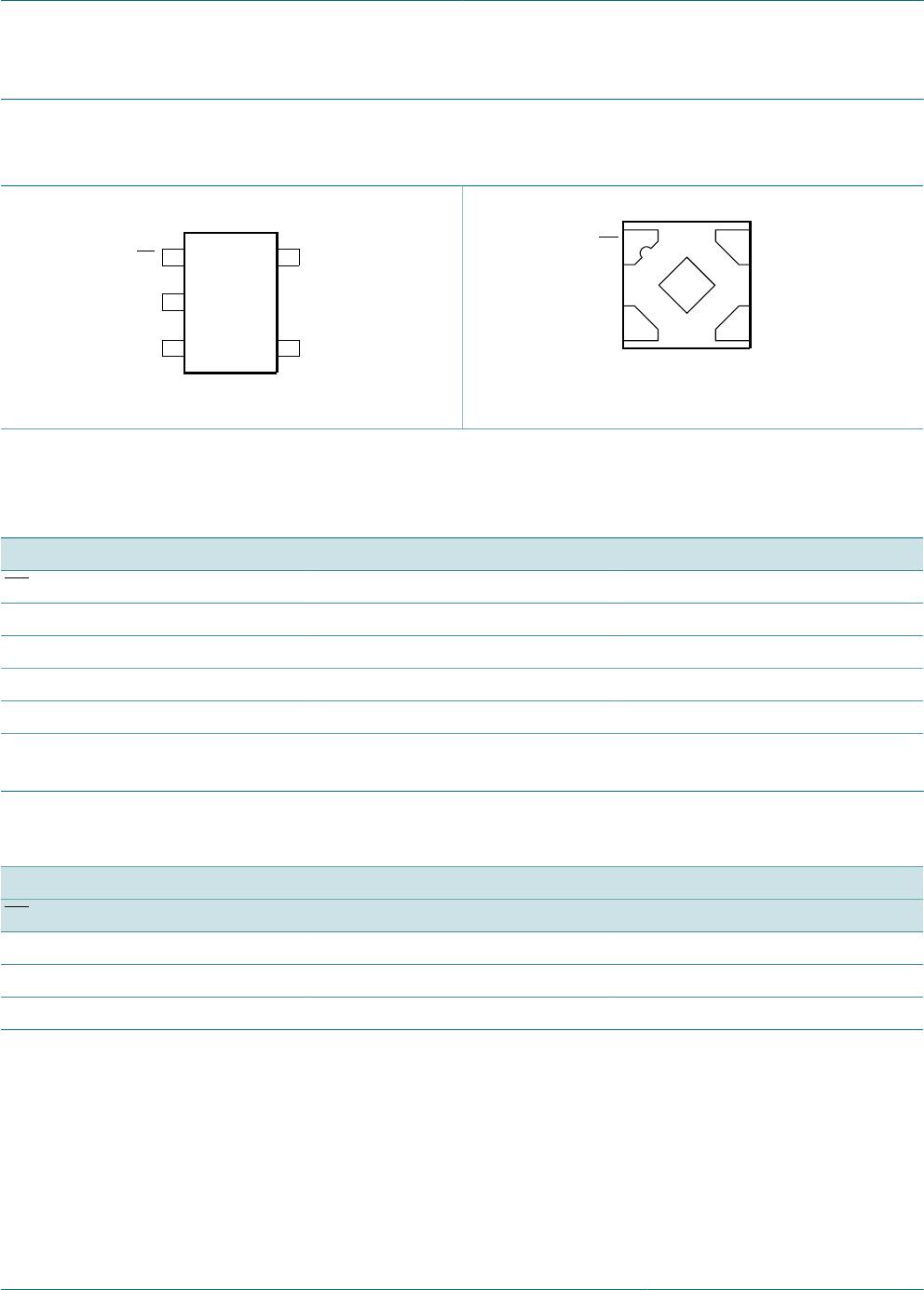
Figure 4.  Pin configuration SOT353-1 (TSSOP5)
OE V
CC
GND
1
3
2
5
4
A
Y
aaa-027740
Transparent top view
74LV1T125
Figure 5.  Pin configuration SOT1226 (X2SON5)
7.2 Pin description
Table 3. Pin description
Symbol Pin Description
OE 1 output enable input
A 2 data input
GND 3 ground (0 V)
Y 4 data output
V
CC
5 supply voltage
8 Functional description
Table 4. Function table
H = HIGH voltage level; L = LOW voltage level; X = don’t care; Z = high-impedance OFF-state.
Input Output
OE A Y
L L L
L H H
H X Z

74LV1T125GWH

Mfr. #:
Manufacturer:
Nexperia
Description:
Translation - Voltage Levels Single supply translating buffer/line driver; 3-state - SOT353 UMT5
Lifecycle:
New from this manufacturer.
Delivery:
DHL FedEx Ups TNT EMS
Payment:
T/T Paypal Visa MoneyGram Western Union

Products related to this Datasheet