MBR20H100CTG, MBRB20H100CTG, MBRF20H100CTG, NRVBB20H100CTT4G
www.onsemi.com
6
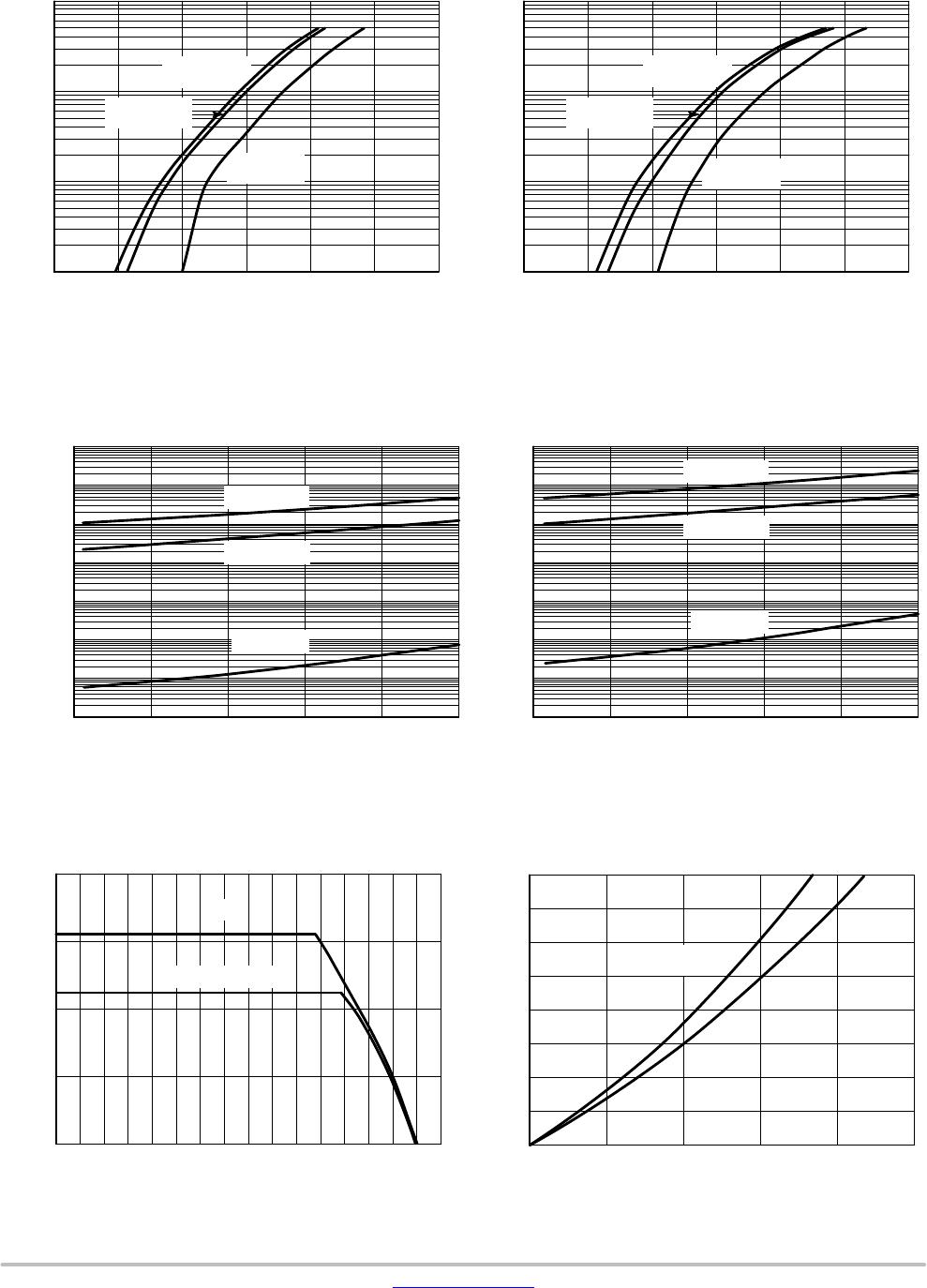
R(t), TRANSIENT THERMAL RESISTANCE
Figure 10. Thermal Response Junction−to−Case for MBRF20H100CT
100
0.10.00001
t
1
, TIME (sec)
0.1
0.0001 0.001 0.01 1 10 1000.000001
0.01
1
10
P
(pk)
t
1
t
2
DUTY CYCLE, D = t
1
/t
2
D = 0.5
SINGLE PULSE
0.2
0.1
0.05
0.01
0.001
MERCURY
SWITCH
V
D
I
D
DUT
10 mH COIL
+V
DD
I
L
S
1
BV
DUT
I
L
I
D
V
DD
t
0
t
1
t
2
t
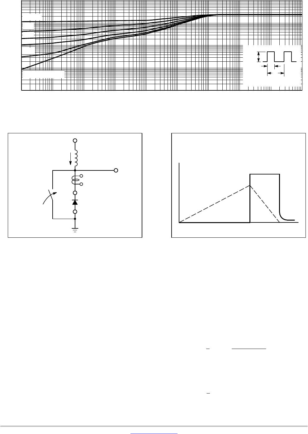
Figure 11. Test Circuit
Figure 12. Current−Voltage Waveforms
The unclamped inductive switching circuit shown in
Figure 11 was used to demonstrate the controlled avalanche
capability of this device. A mercury switch was used instead
of an electronic switch to simulate a noisy environment
when the switch was being opened.
When S
1
is closed at t
0
the current in the inductor I
L
ramps
up linearly; and energy is stored in the coil. At t
1
the switch
is opened and the voltage across the diode under test begins
to rise rapidly, due to di/dt effects, when this induced voltage
reaches the breakdown voltage of the diode, it is clamped at
BV
DUT
and the diode begins to conduct the full load current
which now starts to decay linearly through the diode, and
goes to zero at t
2
.
By solving the loop equation at the point in time when S
1
is opened; and calculating the energy that is transferred to
the diode it can be shown that the total energy transferred is
equal to the energy stored in the inductor plus a finite amount
of energy from the V
DD
power supply while the diode is in
breakdown (from t
1
to t
2
) minus any losses due to finite
component resistances. Assuming the component resistive
elements are small Equation (1) approximates the total
energy transferred to the diode. It can be seen from this
equation that if the V
DD
voltage is low compared to the
breakdown voltage of the device, the amount of energy
contributed by the supply during breakdown is small and the
total energy can be assumed to be nearly equal to the energy
stored in the coil during the time when S
1
was closed,
Equation (2).
W
AVAL
[
1
2
LI
2
LPK
ǒ
BV
DUT
BV
DUT
° V
DD
Ǔ
W
AVAL
[
1
2
LI
2
LPK
EQUATION (1):
EQUATION (2):