LT6109-1/LT6109-2
16
610912fa
If the output current is very low and an input transient
occurs, there may be an increased delay before the
output voltage begins to change. The Typical Performance
Characteristics show that this delay is short and it can
be improved by increasing the minimum output current,
either by increasing R
SENSE
or decreasing R
IN
. Note that
the Typical Performance Characteristics are labeled with
respect to the initial sense voltage.
The speed is also affected by the external components.
Using a larger R
OUT
will decrease the response time, since
V
OUT
= I
OUTA
• Z
OUT
where Z
OUT
is the parallel combination
of R
OUT
and any parasitic and/or load capacitance. Note
that reducing R
IN
or increasing R
OUT
will both have the
effect of increasing the voltage gain of the circuit. If the
output capacitance is limiting the speed of the system, R
IN
and R
OUT
can be decreased together in order to maintain
the desired gain and provide more current to charge the
output capacitance.
The response time of the comparators is the sum of the
propagation delay and the fall time. The propagation
delay is a function of the overdrive voltage on the input
of the comparators. A larger overdrive will result in a
lower propagation delay. This helps achieve a fast system
response time to fault events. The fall time is affected by
the load on the output of the comparator as well as the
pull-up voltage.
The LT6109 amplifier has a typical response time of 500ns
and the comparators have a typical response time of 500ns.
When configured as a system, the amplifier output drives
the comparator input causing a total system response
time which is typically greater than that implied by the
individually specified response times. This is due to the
overdrive on the comparator input being determined by
the speed of the amplifier output.
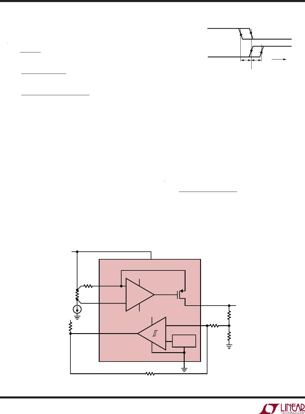
Internal Reference and Comparators
The integrated precision reference and comparators com-
bined with the high precision current sense allow for rapid
and easy detection of abnormal load currents. This is often
critical in systems that require high levels of safety and
reliability. The LT6109 comparators are optimized for fault
detection and are designed with latching outputs. Latch-
ing outputs prevent faults from clearing themselves and
APPLICATIONS INFORMATION
require a separate system or user to reset the outputs. In
applications where the comparator output can intervene
and disconnect loads from the supply, latched outputs are
required to avoid oscillation. Latching outputs are also
useful for detecting problems that are intermittent. The
comparator outputs on the LT6109 are always latching
and there is no way to disable this feature.
Each of the comparators has one input available externally,
with the two versions of the part differing by the polarity
of those available inputs. The other comparator inputs are
connected internally to the 400mV precision reference.
The input threshold (the voltage which causes the output
to transition from high to low) is designed to be equal to
that of the reference. The reference voltage is established
with respect to the device V
–
connection.
Comparator Inputs
The comparator inputs can swing from V
–
to 60V regardless
of the supply voltage used. The input current for inputs
well above the threshold is just a few pAs. With decreas-
ing input voltage, a small bias current begins to be drawn
out of the input near the threshold, reaching 50nA max
when at ground potential. Note that this change in input
bias current can cause a small nonlinearity in the OUTA
transfer function if the comparator inputs are coupled to
the amplifier output with a voltage divider. For example, if
the maximum comparator input current is 50nA, and the
resistance seen looking out of the comparator input is 1k,
then a change in output voltage of 50µV will be seen on the
analog output when the comparator input voltage passes
through its threshold. If both comparator inputs are con-
nected to the output then they must both be considered.
Setting Comparator Thresholds
The comparators have an internal precision 400mV refer-
ence. In order to set the trip points of the LT6109-1 com-
parators, the output currents, I
OVER
and I
UNDER
, as well
as the maximum output current, I
MAX
, must be calculated:
I
OVER
=
V
SENSE(OVER)
R
IN
, I
UNDER
=
V
SENSE(UNDER)
R
IN
,
I
MAX
=
V
SENSE(MAX)
R
IN