LT6109-1/LT6109-2
20
610912fa
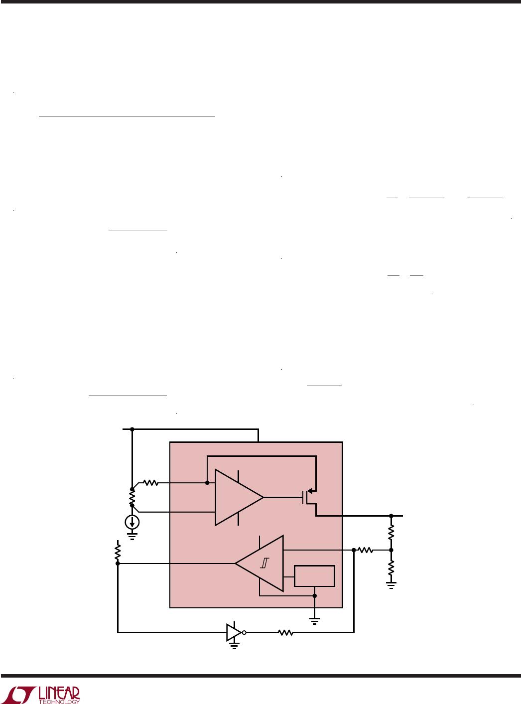
APPLICATIONS INFORMATION
To ensure (R1 + R2) >> R7, R1 should be chosen such
that R1 >> R7 so that V
OUTA
does not change significantly
when the comparator trips.
R3 should be chosen to allow sufficient V
OL
and compara-
tor output rise time due to capacitive loading.
R2 can be calculated:
R2 = R1•
V
DD
– 390mV
V
HYS(EXTRA)
Note that the hysteresis being added, V
HYS(EXTRA)
, is in
addition to the typical 10mV of built-in hysteresis. For very
large values of R2 PCB related leakage may become an
issue. A tee network can be implemented to reduce the
required resistor values.
The approximate total hysteresis is:
V
HYS
= 10mV +R1•
V
DD
– 390mV
R2
For example, to achieve I
OVER
= 900µA with 50mV of total
hysteresis, R7 = 442Ω. Choosing R1 = 4.42k, R3 = 10k
and V
DD
= 5V results in R2 = 513k.
The analog output voltage will also be affected when the
comparator trips due to the current injected into R7 by
the positive feedback. Because of this, it is desirable to
have (R1 + R2) >> R7. The maximum V
OUTA
error caused
by this can be calculated as:
∆V
OUTA
= V
DD
•
R7
R1+R2+R7
In the previous example, this is an error of 4.3mV at the
output of the amplifier or 43µV at the input of the amplifier
assuming a gain of 100.
When using the comparators with their inputs decoupled
from the output of the amplifier they may be driven directly
by a voltage source. It is useful to know the threshold
voltage equations with additional hysteresis. The input
rising edge threshold which causes the output to transi-
tion from high to low is:
V
TH(R)
= 400mV • 1+
R1
R2
The input falling edge threshold which causes the output
to transition from low to high is:
V
TH(F)
= 390mV • 1+
R1
R2
–V
DD
R1
R2
Comparator Outputs
The comparator outputs can maintain a logic low level of
150mV while sinking 500µA. The outputs can sink higher
currents at elevated V
OL
levels as shown in the Typical
Performance Characteristics. Load currents are conducted
to the V
–
pin. The output off-state voltage may range
between 0V and 60V with respect to V
–
, regardless of the
supply voltage used. As with any open-drain device, the
outputs may be tied together to implement wire-OR logic
functions. The LT6109-1 can be used as a single-output
window comparator in this way.
EN/RST Pin
The EN/RST pin performs the two functions of resetting
the latch on the comparators as well as shutting down the
LT6109. After powering on the LT6109, the comparators
must be reset in order to guarantee a valid state at their
outputs.
Applying a pulse to the EN/RST pin will reset the compara-
tors from their tripped state as long as the input on the
comparator is below the threshold and hysteresis for an
inverting comparator or above the threshold and hysteresis
for a noninverting comparator. For example, if V
INC1
is
pulled higher than 400mV and latches the comparator, a
reset pulse will not reset that comparator unless its input
is held below the threshold by a voltage greater than the
10mV typical hysteresis. The comparator outputs typically
unlatch in 0.5µs with 2pF of capacitive load. Increased
capacitive loading will cause increased unlatch time.
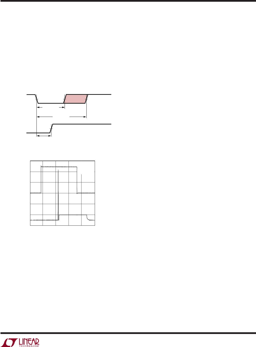
Figure 15 shows the reset functionality of the EN/RST
pin. The width of the pulse applied to reset the compara-
tors must be greater than t
RPW(MIN)
(2µs) but less than
t
RPW(MAX)
(15µs). Applying a pulse that is longer than
40µs typically (or tying the pin low) will cause the part
to enter shutdown. Once the part has entered shutdown,
the supply current will be reduced to 3µA typically and the
amplifier, comparators and reference will cease to function