74LVC161 All information provided in this document is subject to legal disclaimers. © NXP B.V. 2013. All rights reserved.
Product data sheet Rev. 6 — 30 September 2013 4 of 22
NXP Semiconductors
74LVC161
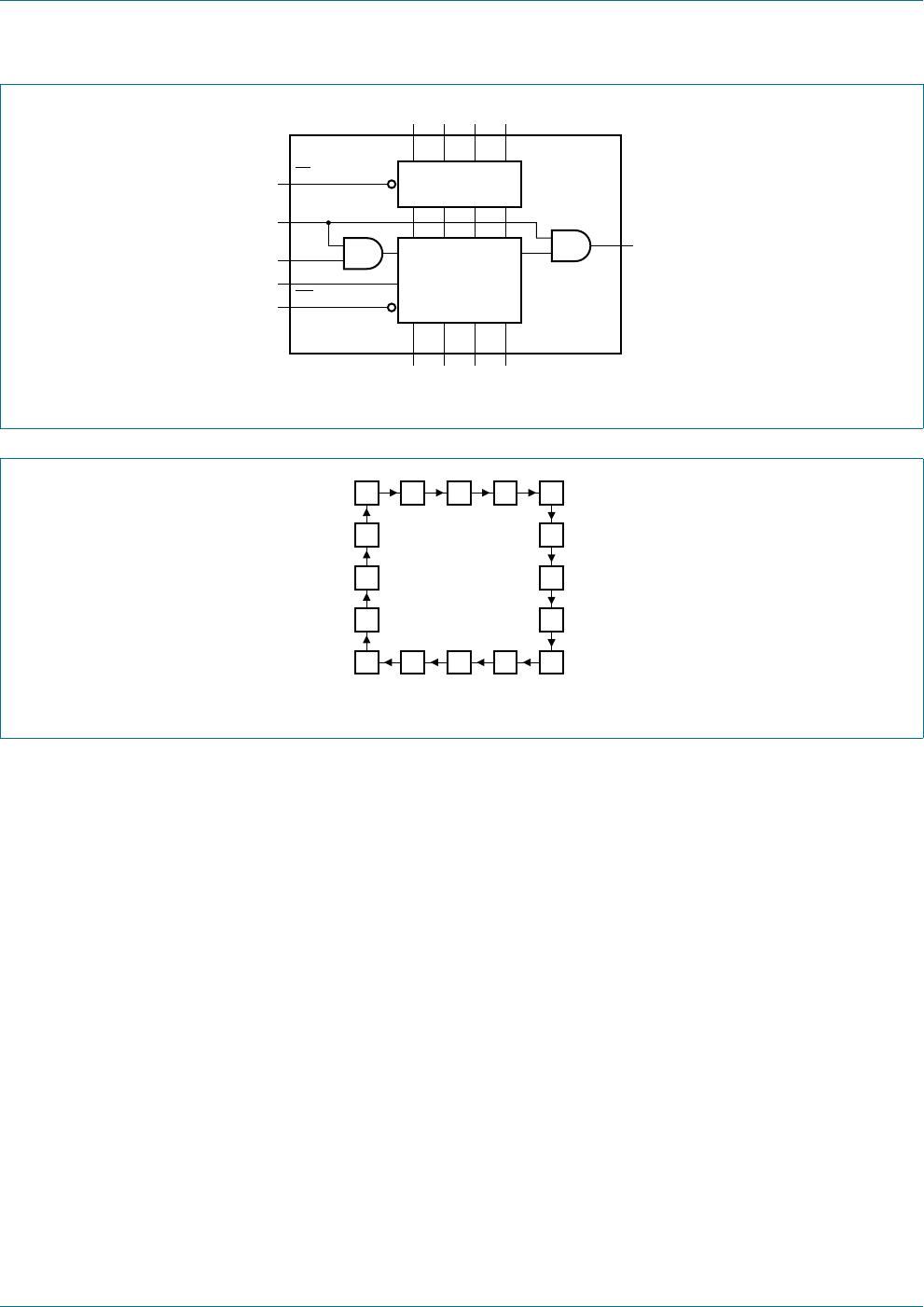
Presettable synchronous 4-bit binary counter; asynchronous reset
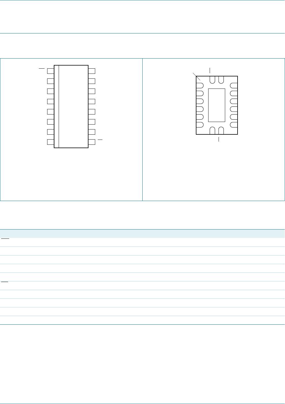
5. Pinning information
5.1 Pinning
5.2 Pin description
(1) This is not a supply pin. The substrate is attached to this
pad using conductive die attach material. There is no
electrical or mechanical requirement to solder this pad.
However, if it is soldered, the solder land should remain
floating or be connected to GND.
Fig 5. Pin configuration for SO16 and (T)SSOP16 Fig 6. Pin configuration for DHVQFN16
161
MR V
CC
CP TC
D0 Q0
D1 Q1
D2 Q2
D3 Q3
CEP CET
GND PE
001aad086
1
2
3
4
5
6
7
8
10
9
12
11
14
13
16
15
001aad087
161
CEP CET
D3 Q3
D2 Q2
D1 Q1
D0 Q0
CP TC
GND
(1)
GND
PE
MR
V
CC
Transparent top view
7 10
6 11
5 12
4
13
3 14
2 15
8
9
1
16
terminal 1
index area
Table 2. Pin description
Symbol Pin Description
MR
1 synchronous master reset (active LOW)
CP 2 clock input (LOW-to-HIGH, edge-triggered)
D[0:3] 3, 4, 5, 6 data input
CEP 7 count enable input
GND 8 ground (0 V)
PE
9 parallel enable input (active LOW)
CET 10 count enable carry input
Q[0:3] 14, 13, 12, 11 flip-flop output
TC 15 terminal count output
V
CC
16 supply voltage