MC74HC151A
www.onsemi.com
6
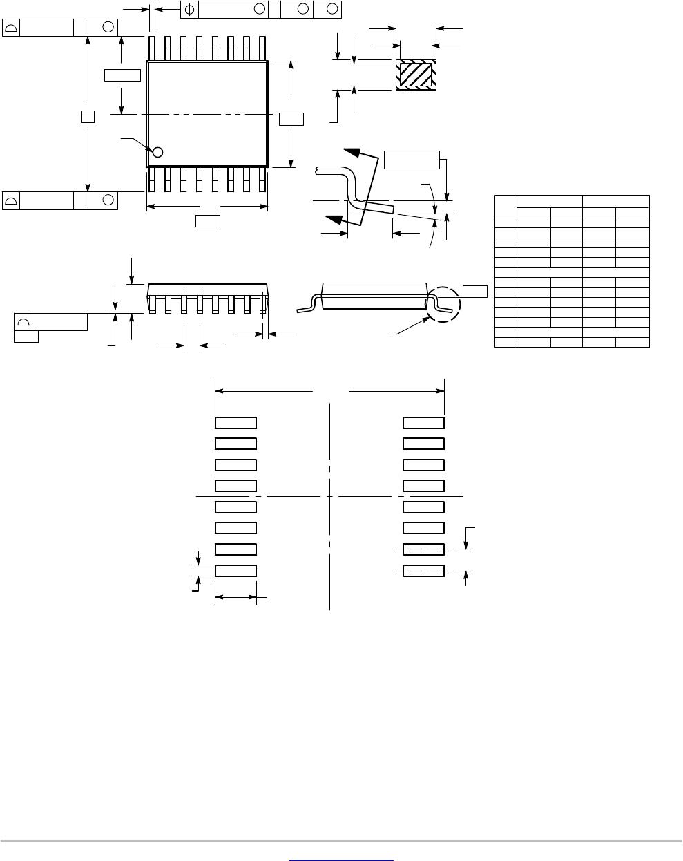
PACKAGE DIMENSIONS
DT SUFFIX
CASE 948F
ISSUE B
DIM MIN MAX MIN MAX
INCHESMILLIMETERS
A 4.90 5.10 0.193 0.200
B 4.30 4.50 0.169 0.177
C −−− 1.20 −−− 0.047
D 0.05 0.15 0.002 0.006
F 0.50 0.75 0.020 0.030
G 0.65 BSC 0.026 BSC
H 0.18 0.28 0.007 0.011
J 0.09 0.20 0.004 0.008
J1 0.09 0.16 0.004 0.006
K 0.19 0.30 0.007 0.012
K1 0.19 0.25 0.007 0.010
L 6.40 BSC 0.252 BSC
M 0 8 0 8
NOTES:
1. DIMENSIONING AND TOLERANCING PER
ANSI Y14.5M, 1982.
2. CONTROLLING DIMENSION: MILLIMETER.
3. DIMENSION A DOES NOT INCLUDE MOLD
FLASH. PROTRUSIONS OR GATE BURRS.
MOLD FLASH OR GATE BURRS SHALL NOT
EXCEED 0.15 (0.006) PER SIDE.
4. DIMENSION B DOES NOT INCLUDE
INTERLEAD FLASH OR PROTRUSION.
INTERLEAD FLASH OR PROTRUSION SHALL
NOT EXCEED 0.25 (0.010) PER SIDE.
5. DIMENSION K DOES NOT INCLUDE
DAMBAR PROTRUSION. ALLOWABLE
DAMBAR PROTRUSION SHALL BE 0.08
(0.003) TOTAL IN EXCESS OF THE K
DIMENSION AT MAXIMUM MATERIAL
CONDITION.
6. TERMINAL NUMBERS ARE SHOWN FOR
REFERENCE ONLY.
7. DIMENSION A AND B ARE TO BE
DETERMINED AT DATUM PLANE −W−.
____
SECTION N−N
SEATING
PLANE
IDENT.
PIN 1
1
8
16
9
DETAIL E
J
J1
B
C
D
A
K
K1
H
G
DETAIL E
F
M
L
2X L/2
−U−
S
U0.15 (0.006) T
S
U0.15 (0.006) T
S
U
M
0.10 (0.004) V
S
T
0.10 (0.004)
−T−
−V−
−W−
0.25 (0.010)
16X REFK
N
N
7.06
16X
0.36
16X
1.26
0.65
DIMENSIONS: MILLIMETERS
1
PITCH
SOLDERING FOOTPRINT*
*For additional information on our Pb−Free strategy and soldering
details, please download the ON Semiconductor Soldering and
Mounting Techniques Reference Manual, SOLDERRM/D.

