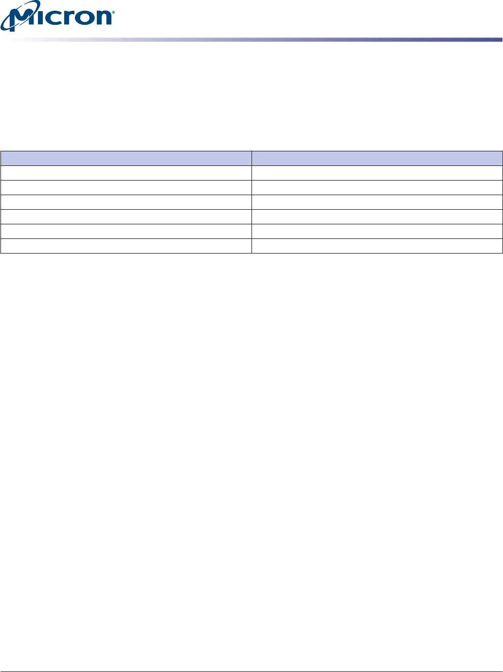
DRAM Operating Conditions
Recommended AC operating conditions are given in the DDR2 component data sheets.
Component specifications are available on Micron's Web site. Module speed grades cor-
relate with component speed grades.
Table 8: Module and Component Speed Grades
DDR2 components may exceed the listed module speed grades; module may not be available in all listed speed grades
Module Speed Grade Component Speed Grade
-1GA -187E
-80E -25E
-800 -25
-667 -3
-53E -37E
-40E -5E
Design Considerations
Simulations
Micron memory modules are designed to optimize signal integrity through carefully de-
signed terminations, controlled board impedances, routing topologies, trace length
matching, and decoupling. However, good signal integrity starts at the system level. Mi-
cron encourages designers to simulate the signal characteristics of the system's memo-
ry bus to ensure adequate signal integrity of the entire memory system.
Power
Operating voltages are specified at the DRAM, not at the edge connector of the module.
Designers must account for any system voltage drops at anticipated power levels to en-
sure the required supply voltage is maintained.
512MB, 1GB (x72, ECC, SR) 244-Pin DDR2 VLP Mini-RDIMM
DRAM Operating Conditions
PDF: 09005aef83d09b45
hvf9c64_128x72pkz.pdf - Rev. C 4/14 EN
10
Micron Technology, Inc. reserves the right to change products or specifications without notice.
© 2009 Micron Technology, Inc. All rights reserved.
IDD Specifications
Table 9: I
DD
Specifications and Conditions – 512MB (Die Revision G)
Values shown for MT47H64M8 DDR2 SDRAM only and are computed from values specified in the 512Mb (64 Meg x 8) com-
ponent data sheet
Parameter/Condition Symbol
-80E
-800 -667 Units
Operating one bank active-precharge current:
t
CK =
t
CK (I
DD
),
t
RC =
t
RC (I
DD
),
t
RAS =
t
RAS MIN (I
DD
); CKE is HIGH, S# is HIGH between valid commands; Address
bus inputs are switching; Data bus inputs are switching
I
DD0
585 540 mA
Operating one bank active-read-precharge current: I
OUT
= 0mA; BL = 4, CL = CL
(I
DD
), AL = 0;
t
CK =
t
CK (I
DD
),
t
RC =
t
RC (I
DD
),
t
RAS =
t
RAS MIN (I
DD
),
t
RCD =
t
RCD (I
DD
);
CKE is HIGH, S# is HIGH between valid commands; Address bus inputs are switching;
Data pattern is same as I
DD4W
I
DD1
675 630 mA
Precharge power-down current: All device banks idle;
t
CK =
t
CK (I
DD
); CKE is LOW;
Other control and address bus inputs are stable; Data bus inputs are floating
I
DD2P
63 63 mA
Precharge quiet standby current: All device banks idle;
t
CK =
t
CK (I
DD
); CKE is
HIGH, S# is HIGH; Other control and address bus inputs are stable; Data bus inputs
are floating
I
DD2Q
216 198 mA
Precharge standby current: All device banks idle;
t
CK =
t
CK (I
DD
); CKE is HIGH, S#
is HIGH; Other control and address bus inputs are switching; Data bus inputs are
switching
I
DD2N
252 225 mA
Active power-down current: All device banks open;
t
CK =
t
CK
(I
DD
); CKE is LOW; Other control and address bus inputs are stable;
Data bus inputs are floating
Fast PDN exit
MR[12] = 0
I
DD3P
162 135 mA
Slow PDN exit
MR[12] = 1
81 81 mA
Active standby current: All device banks open;
t
CK =
t
CK (I
DD
),
t
RAS =
t
RAS MAX
(I
DD
),
t
RP =
t
RP (I
DD
); CKE is HIGH, S# is HIGH between valid commands; Other control
and address bus inputs are switching; Data bus inputs are switching
I
DD3N
297 270 mA
Operating burst write current: All device banks open; Continuous burst writes;
BL = 4, CL = CL (I
DD
), AL = 0;
t
CK =
t
CK (I
DD
),
t
RAS =
t
RAS MAX (I
DD
),
t
RP =
t
RP (I
DD
);
CKE is HIGH, S# is HIGH between valid commands; Address bus inputs are switching;
Data bus inputs are switching
I
DD4W
1125 1035 mA
Operating burst read current: All device banks open; Continuous burst reads; I
OUT
= 0mA; BL = 4, CL = CL (I
DD
), AL = 0;
t
CK =
t
CK (I
DD
),
t
RAS =
t
RAS MAX (I
DD
),
t
RP =
t
RP
(I
DD
); CKE is HIGH, S# is HIGH between valid commands; Address bus inputs are
switching; Data bus inputs are switching
I
DD4R
1080 990 mA
Burst refresh current:
t
CK =
t
CK (I
DD
); REFRESH command at every
t
RFC (I
DD
) inter-
val; CKE is HIGH, S# is HIGH between valid commands; Other control and address bus
inputs are switching; Data bus inputs are switching
I
DD5
855 810 mA
Self refresh current: CK and CK# at 0V; CKE 0.2V; Other control and address bus
inputs are floating; Data bus inputs are floating
I
DD6
63 63 mA
Operating bank interleave read current: All device banks interleaving reads;
I
OUT
= 0mA; BL = 4, CL = CL (I
DD
), AL =
t
RCD (I
DD
) - 1 ×
t
CK (I
DD
);
t
CK =
t
CK (I
DD
),
t
RC =
t
RC (I
DD
),
t
RRD =
t
RRD (I
DD
),
t
RCD =
t
RCD (I
DD
); CKE is HIGH, S# is HIGH between valid
commands; Address bus inputs are stable during deselects; Data bus inputs are
switching
I
DD7
1350 1260 mA
512MB, 1GB (x72, ECC, SR) 244-Pin DDR2 VLP Mini-RDIMM
IDD Specifications
PDF: 09005aef83d09b45
hvf9c64_128x72pkz.pdf - Rev. C 4/14 EN
11
Micron Technology, Inc. reserves the right to change products or specifications without notice.
© 2009 Micron Technology, Inc. All rights reserved.
Table 10: I
DD
Specifications and Conditions – 1GB (Die Revision H)
Values shown for MT47H128M8 DDR2 SDRAM only and are computed from values specified in the 1Gb (128 Meg x 8) com-
ponent data sheet
Parameter/Condition Symbol
-80E
-800 -667 Units
Operating one bank active-precharge current:
t
CK =
t
CK (I
DD
),
t
RC =
t
RC (I
DD
),
t
RAS =
t
RAS MIN (I
DD
); CKE is HIGH, S# is HIGH between valid commands; Address
bus inputs are switching; Data bus inputs are switching
I
DD0
585 540 mA
Operating one bank active-read-precharge current: I
OUT
= 0mA; BL = 4, CL = CL
(I
DD
), AL = 0;
t
CK =
t
CK (I
DD
),
t
RC =
t
RC (I
DD
),
t
RAS =
t
RAS MIN (I
DD
),
t
RCD =
t
RCD (I
DD
);
CKE is HIGH, S# is HIGH between valid commands; Address bus inputs are switching;
Data pattern is same as I
DD4W
I
DD1
675 630 mA
Precharge power-down current: All device banks idle;
t
CK =
t
CK (I
DD
); CKE is LOW;
Other control and address bus inputs are stable; Data bus inputs are floating
I
DD2P
63 63 mA
Precharge quiet standby current: All device banks idle;
t
CK =
t
CK (I
DD
); CKE is
HIGH, S# is HIGH; Other control and address bus inputs are stable; Data bus inputs
are floating
I
DD2Q
216 216 mA
Precharge standby current: All device banks idle;
t
CK =
t
CK (I
DD
); CKE is HIGH, S#
is HIGH; Other control and address bus inputs are switching; Data bus inputs are
switching
I
DD2N
252 216 mA
Active power-down current: All device banks open;
t
CK =
t
CK
(I
DD
); CKE is LOW; Other control and address bus inputs are stable;
Data bus inputs are floating
Fast PDN exit
MR[12] = 0
I
DD3P
180 135 mA
Slow PDN exit
MR[12] = 1
90 90 mA
Active standby current: All device banks open;
t
CK =
t
CK (I
DD
),
t
RAS =
t
RAS MAX
(I
DD
),
t
RP =
t
RP (I
DD
); CKE is HIGH, S# is HIGH between valid commands; Other control
and address bus inputs are switching; Data bus inputs are switching
I
DD3N
297 270 mA
Operating burst write current: All device banks open; Continuous burst writes;
BL = 4, CL = CL (I
DD
), AL = 0;
t
CK =
t
CK (I
DD
),
t
RAS =
t
RAS MAX (I
DD
),
t
RP =
t
RP (I
DD
);
CKE is HIGH, S# is HIGH between valid commands; Address bus inputs are switching;
Data bus inputs are switching
I
DD4W
1125 1035 mA
Operating burst read current: All device banks open; Continuous burst reads; I
OUT
= 0mA; BL = 4, CL = CL (I
DD
), AL = 0;
t
CK =
t
CK (I
DD
),
t
RAS =
t
RAS MAX (I
DD
),
t
RP =
t
RP
(I
DD
); CKE is HIGH, S# is HIGH between valid commands; Address bus inputs are
switching; Data bus inputs are switching
I
DD4R
1080 990 mA
Burst refresh current:
t
CK =
t
CK (I
DD
); REFRESH command at every
t
RFC (I
DD
) inter-
val; CKE is HIGH, S# is HIGH between valid commands; Other control and address bus
inputs are switching; Data bus inputs are switching
I
DD5
1305 1260 mA
Self refresh current: CK and CK# at 0V; CKE 0.2V; Other control and address bus
inputs are floating; Data bus inputs are floating
I
DD6
63 63 mA
Operating bank interleave read current: All device banks interleaving reads;
I
OUT
= 0mA; BL = 4, CL = CL (I
DD
), AL =
t
RCD (I
DD
) - 1 ×
t
CK (I
DD
);
t
CK =
t
CK (I
DD
),
t
RC =
t
RC (I
DD
),
t
RRD =
t
RRD (I
DD
),
t
RCD =
t
RCD (I
DD
); CKE is HIGH, S# is HIGH between valid
commands; Address bus inputs are stable during deselects; Data bus inputs are
switching
I
DD7
1890 1665 mA
512MB, 1GB (x72, ECC, SR) 244-Pin DDR2 VLP Mini-RDIMM
IDD Specifications
PDF: 09005aef83d09b45
hvf9c64_128x72pkz.pdf - Rev. C 4/14 EN
12
Micron Technology, Inc. reserves the right to change products or specifications without notice.
© 2009 Micron Technology, Inc. All rights reserved.

MT9HVF12872PKZ-80EH1

Mfr. #:
Manufacturer:
Micron
Description:
DRAM Module DDR2 SDRAM 1Gbyte 244MiniRDIMM
Lifecycle:
New from this manufacturer.
Delivery:
DHL FedEx Ups TNT EMS
Payment:
T/T Paypal Visa MoneyGram Western Union

Products related to this Datasheet