DS1110LE-200+

General Description
The DS1110L 10-tap delay line is a 3V version of the
DS1110. It has 10 equally spaced taps providing delays
from 10ns to 500ns. The DS1110L series delay lines
provide a nominal accuracy of ±5% or ±2ns, whichever
is greater, at 3.3V and +25°C. The DS1110L is character-
ized to operate from 2.7V to 3.6V. The DS1110L
produces both leading- and trailing-edge delays with
equal precision. The device is offered in a standard
14-pin TSSOP.
Features
All-Silicon Delay Line
3V Version of the DS1110
10 Taps Equally Spaced
Delays Are Stable and Precise
Leading- and Trailing-Edge Accuracy
Delay Tolerance ±5% or ±2ns, Whichever Is
Greater, at 3.3V and +25°C
Economical
Low-Profile 14-Pin TSSOP
Low-Power CMOS
TTL/CMOS Compatible
Vapor Phase and IR Solderable
Fast-Turn Prototypes
Delays Specified Over Commercial and Industrial
Temperature Ranges
Custom Delays Available
DS1110L
3V 10-Tap Silicon Delay Line
_____________________________________________ Maxim Integrated Products 1
14
13
12
11
10
9
8
1
2
3
4
5
6
7
V
CC
TAP1
TAP3
TAP5TAP4
TAP2
N.C.
IN
TOP VIEW
TAP7
TAP9
TAP10GND
TAP8
TAP6
TSSOP (173mil)
DS1110L
Pin Configuration
Ordering Information
XX-XXXX; Rev 1; 11/03
For pricing, delivery, and ordering information, please contact Maxim/Dallas Direct! at
1-888-629-4642, or visit Maxim’s website at www.maxim-ic.com.
PART
TEM P RANGE
PIN-
PACKAGE
TOTAL
DELAY
( ns) *
DS1110LE-100
-40°C to +85°C 14 TSSOP (173mil)
100
DS1110LE-125
-40°C to +85°C 14 TSSOP (173mil)
125
DS1110LE-150
-40°C to +85°C 14 TSSOP (173mil)
150
DS1110LE-175
-40°C to +85°C 14 TSSOP (173mil)
175
DS1110LE-200
-40°C to +85°C 14 TSSOP (173mil)
200
DS1110LE-250
-40°C to +85°C 14 TSSOP (173mil)
250
DS1110LE-300
-40°C to +85°C 14 TSSOP (173mil)
300
DS1110LE-350
-40°C to +85°C 14 TSSOP (173mil)
350
DS1110LE-400
-40°C to +85°C 14 TSSOP (173mil)
400
DS1110LE-450
-40°C to +85°C 14 TSSOP (173mil)
450
DS1110LE-500
-40°C to +85°C 14 TSSOP (173mil)
500
*Custom delays are available.
Applications
Communications Equipment
Medical Devices
Automated Test Equipment
PC Peripheral Devices
DS1110L
3V 10-Tap Silicon Delay Line
2 ______________________________________________________________________
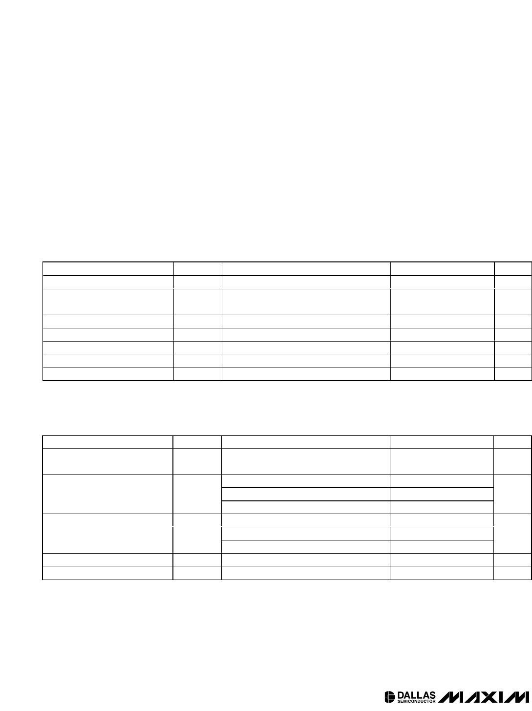
ABSOLUTE MAXIMUM RATINGS
DC ELECTRICAL CHARACTERISTICS
(-40°C to +85°C, V
CC
= 2.7V to 3.6V.)
Stresses beyond those listed under “Absolute Maximum Ratings” may cause permanent damage to the device. These are stress ratings only, and functional
operation of the device at these or any other conditions beyond those indicated in the operational sections of the specifications is not implied. Exposure to
absolute maximum rating conditions for extended periods may affect device reliability.
Voltage on Any Pin Relative to Ground .................-0.5V to +6.0V
Operating Temperature Range ...........................-40°C to +85°C
Storage Temperature Range .............................-55°C to +125°C
Soldering Temperature...................See IPC/JEDEC J-STD-020A
PARAMETER SYMBOL CONDITIONS MIN TYP MAX UNITS
Supply Voltage V
CC
(Note 1) 2.7 3.3 3.6 V
High-Level Input Voltage V
IH
(Note 1) 2.2
V
CC
+ 0.3
V
Low-Level Input Voltage V
IL
(Note 1) -0.3 +0.8 V
Input Leakage Current I
I
0V V
I
V
CC
-1.0 +1.0 µA
Active Current I
CC
V
CC
= max, period = min (Note 2) 40 150 mA
High-Level Output Current I
OH
V
CC
= min, V
OH
= 2.3V -1.0 mA
Low-Level Output Current I
OL
V
CC
= min, V
OL
= 0.5V 12 mA
AC ELECTRICAL CHARACTERISTICS
(-40°C to +85°C, V
CC
= 2.7V to 3.6V.)
PARAMETER SYMBOL CONDITIONS MIN TYP MAX UNITS
Input Pulse Width t
WI
(Note 6)
10% of
tap 10
ns
+25°C, 3.3V (Notes 3, 5, 6, 7, 9) -2 Table 1 +2
0°C to +70°C (Notes 4–7) -3 Table 1 +3
Input to Tap Delay
(Delays
40ns)
t
PLH
t
PHL
-40°C to +85°C (Notes 4–7) -4 Table 1 +4
ns
+25°C, 3.3V (Notes 3, 5, 6, 7, 9) -5 Table 1 +5
0°C to +70°C (Notes 4–7) -8 Table 1 +8
Input to Tap Delay
(Delays > 40ns)
t
PLH
t
PHL
-40°C to +85°C (Notes 4–7) -13 Table 1 +13
%
Power-Up Time t
PU
100 ms
Input Period Period (Note 8) 2 (t
WI
)ns
DS1110L
3V 10-Tap Silicon Delay Line
_____________________________________________________________________ 3
Note 1: All voltages are referenced to ground.
Note 2: Measured with outputs open.
Note 3: Initial tolerances are ± with respect to the nominal value at +25°C and V
CC
= 3.3V for both leading and trailing edges.
Note 4: Temperature and voltage tolerances are with respect to the nominal delay value over stated temperature range and a 2.7V to
3.6V range.
Note 5: Intermediate delay values are available on a custom basis.
Note 6: See Test Conditions section.
Note 7: All tap delays tend to vary unidirectionally with temperature or voltage changes. For example, if tap 1 slows down, all other
taps also slow down; tap 3 can never be faster than tap 2.
Note 8: Pulse width and period specifications may be exceeded; however, accuracy is application sensitive (decoupling, layout, etc.).
Note 9: For Tap 1 delays greater than 20ns, the tolerance is ±3ns or ±5%, whichever is greater.
CAPACITANCE
(T
A
= +25°C.)
Typical Operating Characteristics
(V
CC
= 3.3V, T
A
= +25°C, unless otherwise noted.)
PARAMETER SYMBOL
CONDITIONS
MIN TYP MAX UNITS
Input Capacitance C
IN
510pF
-2
-1
0
1
2
3
4
-3
CHANGE IN DELAY (%) vs. TEMPERATURE
DS1110L-250
DS1110L toc04
TEMPERATURE (°C)
CHANGE IN DELAY (%)
603510-15-40 85
RISING EDGE
FALLING EDGE
CHANGE IN DELAY (%) vs. TEMPERATURE
DS1110L-500
DS1110L toc03
TEMPERATURE (°C)
CHANGE IN DELAY (%)
603510-15
-4
-3
-2
-1
0
1
2
3
4
5
6
-5
-40 85
RISING EDGE
FALLING EDGE
-0.3
-0.2
-0.1
0
0.1
0.2
0.3
-0.4
DELAY CHANGE (%)
vs. V
CC
DS1110L-250
DS1110L toc02
V
CC
(V)
CHANGE IN DELAY (%)
3.33.02.7 3.6
RAISING EDGE
FALLING EDGE
DELAY CHANGE (%)
vs. V
CC
DS1110L-500
DS1110L toc01
V
CC
(V)
CHANGE IN DELAY (%)
3.33.0
-0.30
-0.25
-0.20
-0.15
-0.10
-0.05
0
0.05
0.10
-0.35
2.7 3.6
RAISING EDGE
FALLING EDGE

DS1110LE-200+

Mfr. #:
Manufacturer:
Maxim Integrated
Description:
Delay Lines / Timing Elements 3V 10-Tap Silicon Delay Line
Lifecycle:
New from this manufacturer.
Delivery:
DHL FedEx Ups TNT EMS
Payment:
T/T Paypal Visa MoneyGram Western Union