MAX16000–MAX16007
Low-Voltage, Quad-/Hex-/Octal-Voltage
µP Supervisors
4
Maxim Integrated
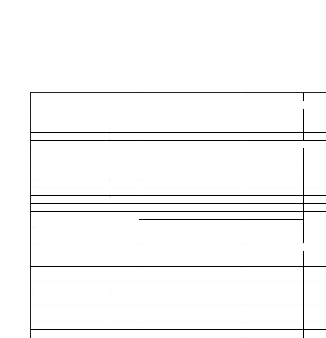
PARAMETER SYMBOL CONDITIONS MIN TYP MAX UNITS
REFERENCE OUTPUT (MAX16005 Only)
Reference Short-Circuit Current Shorted to GND 0.8 mA
Reference Output Accuracy V
REF
No load 1.200 1.235 1.270 V
Line Regulation 0.005 % / V
Reference Load Regulation Sourcing, 0 ≤ I
REF
≤ 40µA 10 Ω
WATCHDOG TIMER (MAX16001/MAX16002/MAX16004–MAX16007)
WDI Input-Voltage Low V
IL
0.3 x
V
CC
V
WDI Input-Voltage High V
IH
0.7 x
V
CC
V
WDI Pulse Width (Note 5) 50 ns
Watchdog Timeout Period t
WDI
1.12 1.6 2.40 s
Watchdog Startup Period MAX16001/2/4/6/7 35 54 72 s
Watchdog Input Current V
WDI
= 0 to V
CC
(Note 5) -1 +1 µA
V
CC
= 3.3V, I
SINK
= 2mA 0.30
WDO Output-Voltage Low
(MAX16005 Only)
V
OL
V
CC
= 2.5V, I
SINK
= 1.2mA 0.30
V
WDO Output-Voltage High
(MAX16005 Only)
V
OH
V
CC
≥ 2.0V, I
SOURCE
= 6µA, WDO
deasserted
0.8 x
V
CC
V
DIGITAL LOGIC
TOL Input-Voltage Low V
IL
0.3 x
V
CC
V
TOL Input-Voltage High V
IH
0.7 x
V
CC
V
TOL Input Current TOL = V
CC
100 nA
MARGIN Input-Voltage Low V
IL
0.3 x
V
CC
V
MARGIN Input-Voltage High V
IH
0.7 x
V
CC
V
MARGIN Pullup Resistance Pulled up to V
CC
12 20 28 kΩ
MARGIN Delay Time t
MD
Rising or falling (Note 6) 50 µs
ELECTRICAL CHARACTERISTICS (continued)
(V
CC
= 2.0V to 5.5V, T
A
= -40°C to +125°C, unless otherwise specified. Typical values are at V
CC
= 3.3V, T
A
= +25°C). (Note 1)
Note 1: Devices are tested at T
A
= +25°C and guaranteed by design for T
A
= T
MIN
to T
MAX
.
Note 2: The outputs are guaranteed to be in the correct logic state down to V
CC
= 1V.
Note 3: Measured with WDI, MARGIN, and MR unconnected.
Note 4: The minimum and maximum specifications for this parameter are guaranteed by using the worst case of the SRT ramp cur-
rent and SRT threshold specifications.
Note 5: Guaranteed by design and not production tested.
Note 6: Amount of time required for logic to lock/unlock outputs from margin testing.

