6.42
IDT7133SA/LA, IDT7143SA/LA
High-Speed 2K x 16 Dual-Port RAM Military, Industrial and Commercial Temperature Ranges
10
AC Electrical Characteristics Over the
Operating Temperature and Supply Voltage
(6)
NOTES:
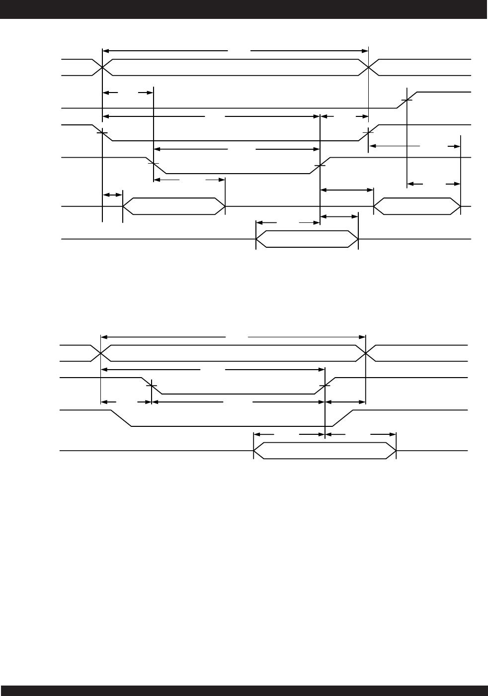
1. Port-to-port delay through RAM cells from writing port to reading port, refer to “Timing Waveform of Write with Port-to-Port Read and Busy".
2. t
BDD is calculated parameter and is greater of 0, tWDD - tWP (actual) or tDDD - tDW (actual).
3. To ensure that the earlier of the two ports wins.
4. To ensure that the write cycle is inhibited on port "B" during contention on port "A".
5. To ensure that a write cycle is completed on port "B" after contention on port "A".
6. 'X' in part number indicates power rating (SA or LA).
7133X20
7143X20
Com'l Only
7133X25
7143X25
Com'l & Ind
7133X35
7143X35
Com'l
& Military
Symbol Parameter Min.Max.Min.Max.Min.Max.Unit
BUSY TIMING (For MASTER 71V33)
t
BAA
BUSY Access Time from Address
____
20
____
20
____
30 ns
t
BDA
BUSY Disable Time from Address
____
20
____
20
____
30 ns
t
BAC
BUSY Access Time from Chip Enable
____
20
____
20
____
25 ns
t
BDC
BUSY Disable Time from Chip Enable
____
17
____
20
____
25 ns
t
WDD
Write Pulse to Data Delay
(1)
____
40
____
50
____
60 ns
t
DDD
Write Data Valid to Read Data Delay
(1)
____
30
____
35
____
45 ns
t
BDD
BUSY Disable to Valid Data
(2)
____
25
____
30
____
35 ns
t
APS
Arbitration Priority Set-up Time
(3)
5
____
5
____
5
____
ns
t
WH
Write Hold After BUSY
(5)
20
____
20
____
25
____
ns
BUSY INPUT TIMING (For SLAVE 71V43)
t
WB
BUSY Inp ut to Write
(4)
0
____
0
____
0
____
ns
t
WH
Write Hold After BUSY
(5)
20
____
20
____
25
____
ns
t
WDD
Write Pulse to Data Delay
(1)
____
40
____
50
____
60 ns
t
DDD
Write Data Valid to Read Data Delay
(1)
____
30
____
35
____
45 ns
2746 tbl 12a
7133X45
7143X45
Com'l Only
7133X55
7143X55
Com'l, Ind
& Military
7133X70/90
7143X70/90
Com'l &
Military
Symbol Parameter Min.Max.Min.Max.Min.Max.Unit
BUSY TIMING (For MASTER 71V33)
t
BAA
BUSY Access Time from Address
____
40
____
40
____
45/45 ns
t
BDA
BUSY Disable Time from Address
____
40
____
40
____
45/45 ns
t
BAC
BUSY Access Time from Chip Enable
____
30
____
35
____
35/35 ns
t
BDC
BUSY Disable Time from Chip Enable
____
25
____
30
____
30/30 ns
t
WDD
Write Pulse to Data Delay
(1)
____
80
____
80
____
90/90 ns
t
DDD
Write Data Valid to Read Data De lay
(1)
____
55
____
55
____
70/70 ns
t
BDD
BUSY Disable to Valid Data
(2)
____
40
____
40
____
40/40 ns
t
APS
Arbitration Priority Se t-up Time
(3)
5
____
5
____
5/5
____
ns
t
WH
Write Hold After BUSY
(5)
30
____
30
____
30/30
____
ns
BUSY INPUT TIMING (For SLAVE 71V43)
t
WB
BUSY Inp ut to Write
(4)
0
____
0
____
0/0
____
ns
t
WH
Write Hold After BUSY
(5)
30
____
30
____
30/30
____
ns
t
WDD
Write Pulse to Data Delay
(1)
____
80
____
80
____
90/90 ns
t
DDD
Write Data Valid to Read Data De lay
(1)
____
55
____
55
____
70/70 ns
2746 tbl 12b