LTC6993-1/LTC6993-2
LTC6993-3/LTC6993-4
19
69931234fc
For more information www.linear.com/LTC6993-1
applicaTions inForMaTion
Table 2. Typical Supply Current
CONDITION TYPICAL I
S(IDLE)
TYPICAL ∆I
S(ACTIVE)
*
N
DIV
≤ 64
V
+
N
DIV
7pF + 4pF
( )
t
OUT
+
V
+
500kΩ
+ 2.2 I
SET
+ 5
0µA
V
+
Duty Cycle
t
OUT
N
DIV
5pF + 18pF + C
L
OAD
(
)
N
DIV
≥ 512
V
+
N
DIV
7pF
t
OUT
+
V
+
500kΩ
+1.8 I
SET
+ 5
0µA
V
+
Duty Cycle
t
OUT
C
LO
AD
*Ignoring resistive loads (assumes R
LOAD
= )
Power Supply Current
The Electrical Characteristics table specifies the supply
current while the part is idle (waiting to be triggered).
I
S(IDLE)
varies with the programmed t
OUT
and the supply
voltage. Once triggered, the instantaneous supply current
increases to I
S(ACTIVE)
while the timing circuit is active.
I
S(ACTIVE)
= I
S(IDLE)
+ I
S(ACTIVE)
The average increase in supply current I
S(ACTIVE)
de-
pends on the output duty cycle (or negative duty cycle,
if POL
= 1), since that represents the percentage of time
that the circuit is active. I
S(IDLE)
and I
S(ACTIVE)
can be
estimated using the equations in Table 2.
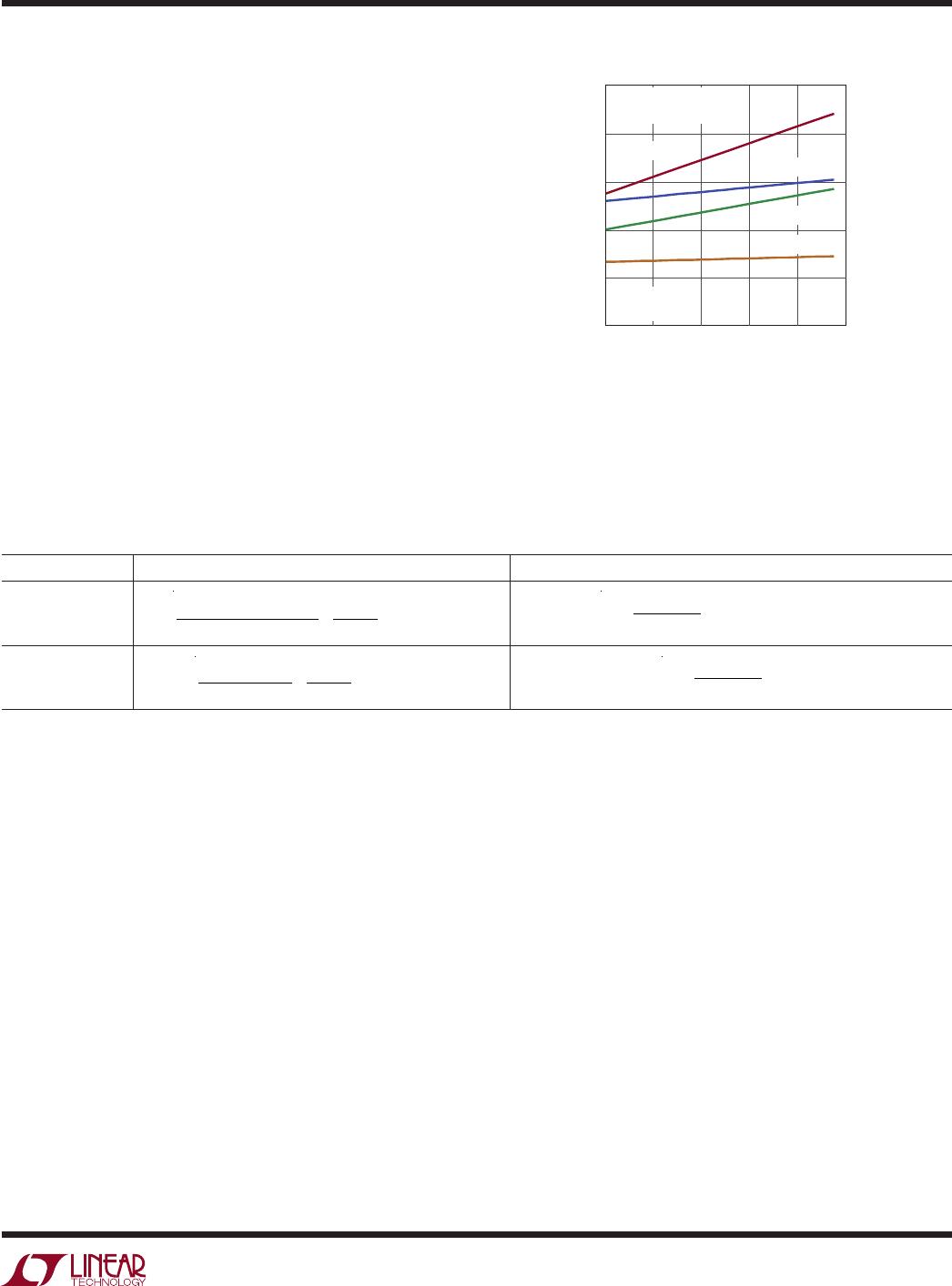
Figure 12 shows how the supply current increases from
I
S(IDLE)
as the input frequency increases. The increase is
smaller at higher N
DIV
settings.
DUTY CYCLE (%)
IDLE
POWER SUPPLY CURRENT (µA)
150
200
250
80
69931234 F12
100
50
0
20
40
60
100
V
+
= 3.3V
DUTY CYCLE = f
IN
• t
OUT
÷1, R
SET
= 50k
÷8, R
SET
= 50k
÷1, R
SET
= 100k
÷1, R
SET
= 800k
C
LOAD
= 5pF
R
LOAD
= ∞
Figure 12. I
S(ACTIVE)
vs Output Duty Cycle
LTC6993-1/LTC6993-2
LTC6993-3/LTC6993-4
20
69931234fc
For more information www.linear.com/LTC6993-1
Supply Bypassing and PCB Layout Guidelines
The LTC6993 is an accurate monostable multivibrator when
used in the appropriate manner. The part is simple to use
and by following a few rules, the expected performance
is easily achieved. Adequate supply bypassing and proper
PCB layout are important to ensure this.
Figure 13 shows example PCB layouts for both the SOT-23
and DCB packages using 0603 sized passive components.
The layouts assume a two layer board with a ground plane
layer beneath and around the LTC6993. These layouts are
a guide and need not be followed exactly.
1. Connect the bypass capacitor, C1, directly to the V
+
and
GND pins using a low inductance path. The connection
from C1 to the V
+
pin is easily done directly on the top
layer. For the DCB package, C1’s connection to GND is
also simply done on the top layer. For the SOT-23, OUT
can be routed through the C1 pads to allow a good C1
GND connection. If the PCB design rules do not allow
that, C1s GND connection can be accomplished through
multiple vias to the ground plane. Multiple vias for both
the GND pin connection to the ground plane and the
C1 connection to the ground plane are recommended
to minimize the inductance. Capacitor C1 should be a
0.1µF ceramic capacitor.
2. Place all passive components on the top side of the
board. This minimizes trace inductance.
3. Place R
SET
as close as possible to the SET pin and
make a direct, short connection. The SET pin is a cur-
rent summing node and currents injected into this pin
d
ir
ectly modulate the output pulse width. Having a short
connection minimizes the exposure to signal pickup.
4. Connect R
SET
directly to the GND pin. Using a long path
or vias to the ground plane will not have a significant
affect on accuracy, but a direct, short connection is
recommended and easy to apply.
5. Use a ground trace to shield the SET pin. This provides
another layer of protection from radiated signals.
6. Place R1 and R2 close to the DIV pin. A direct, short
connection to the DIV pin minimizes the external signal
coupling.
69931234 F13
LTC6993
TRIG
GND
SET
OUT
V
+
DIV
C1
0.1µF
R1
R2
R
SET
V
+
V
+
DIV
SET
OUT
GND
TRIG
C1R1
R2
V
+
R
SET
DCB PACKAGE
TRIG
GND
SET
OUT
V
+
DIV
R2
V
+
R
SET
TSOT-23 PACKAGE
R1
C1
Figure 13. Supply Bypassing and PCB Layout
applicaTions inForMaTion
LTC6993-1/LTC6993-2
LTC6993-3/LTC6993-4
21
69931234fc
For more information www.linear.com/LTC6993-1
Typical applicaTions
Missing Pulse Detector
LTC6993-2
TRIG
GND
SET
OUT
V
+
DIV
R1
102k
DIVCODE = 14
(N
DIV
= 8, POL = 1)
69931234 TA02a
3.3V
0.1µF
R2
976k
R
SET
402k
TRIG
2V/DIV
OUT
2V/DIV
50µs/DIV
69931234 TA02b
25kHz INPUT
64µs
Use retriggerable one shot with output inverted. Output remains low as long as retrigger occurs within t
OUT
= 64µs.
RESET = OPEN
RUN = GND (CLOSED)
20ms
FRAME RATE
GENERATOR
1.5ms
REFERENCE
PULSE
5V
20ms PERIOD
5V
R4
976k
R7
10k
C1
0.01µF
R5
102k
R3
121k
5V
R1
1M
C2
0.01µF
1.5ms PULSE
1.5ms CAL TRIM
69931234 TA03
R2
280k
R8
143k
R6
10k
LTC6991
OUT
V
+
DIV
RST
GND
SET
LTC6993-1
OUT
V
+
DIV
TRIG
GND
SET
1.5ms Radio Control Servo Reference Pulse Generator
PULSE IN
10µs
OUTPUT PULSE
GENERATOR
100µs
DELAY
GENERATOR
5V
R4
182k
C1
0.01µF
C2
0.1µF
R5
976k
R6
78.7k
10µs PULSE IN
10µs PULSE OUT
100µs DELAY
OUT
LTC6993-1
OUT
V
+
DIV
TRIG
GND
SET
5V
R1
976k
R2
102k
R3
61.9k
LTC6993-1
OUT
V
+
DIV
TRIG
GND
SET
Pulse Delay Generator

LTC6993HS6-2#TRMPBF

Mfr. #:
Manufacturer:
Analog Devices Inc.
Description:
Monostable Multivibrator One Shot with Rising Edge Trigger, Retreggerable
Lifecycle:
New from this manufacturer.
Delivery:
DHL FedEx Ups TNT EMS
Payment:
T/T Paypal Visa MoneyGram Western Union