Chapter 3: DC and Switching Characteristics for MAX V Devices 3–11
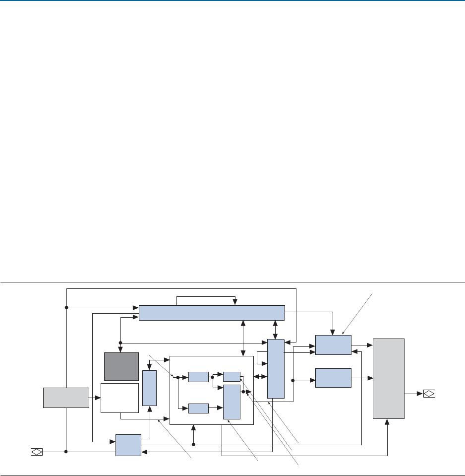
Timing Model and Specifications
May 2011 Altera Corporation MAX V Device Handbook
Preliminary and Final Timing
This section describes the performance, internal, external, and UFM timing
specifications. All specifications are representative of the worst-case supply voltage
and junction temperature conditions.
Timing models can have either preliminary or final status. The Quartus II software
issues an informational message during the design compilation if the timing models
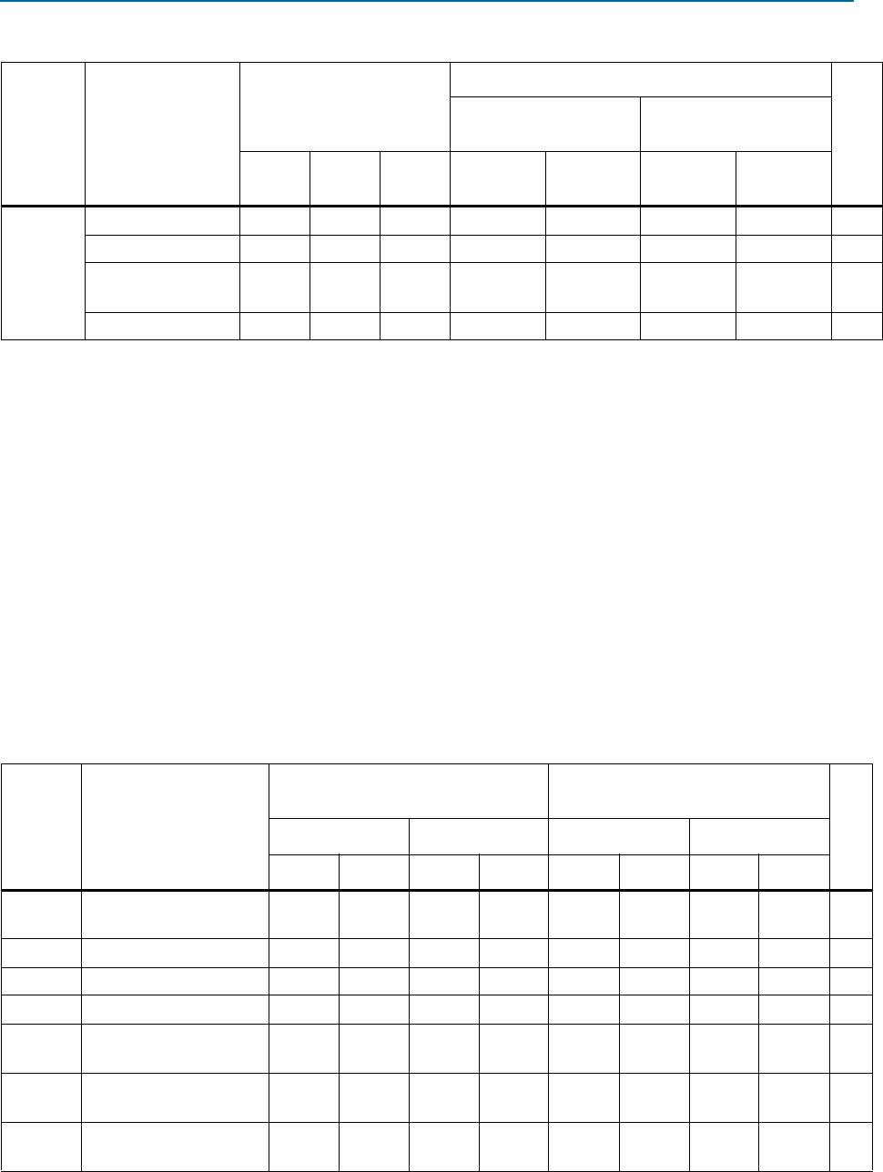
are preliminary. Table 3–16 lists the status of the MAX V device timing models.
Preliminary status means the timing model is subject to change. Initially, timing
numbers are created using simulation results, process data, and other known
parameters. These tests are used to make the preliminary numbers as close to the
actual timing parameters as possible.
Final timing numbers are based on actual device operation and testing. These
numbers reflect the actual performance of the device under the worst-case voltage
and junction temperature conditions.
Performance
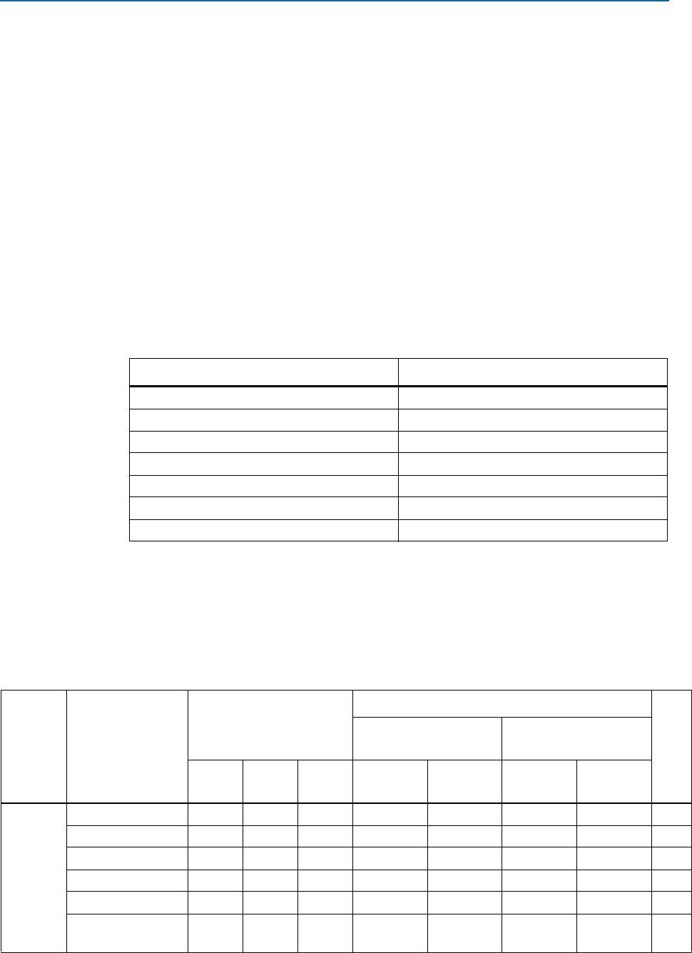
Table 3–17 lists the MAX V device performance for some common designs. All
performance values were obtained with the Quartus II software compilation of
megafunctions.
Table 3–16. Timing Model Status for MAX V Devices
Device Final
5M40Z v
5M80Z v
5M160Z v
5M240Z v
5M570Z v
5M1270Z v
5M2210Z v
Table 3–17. Device Performance for MAX V Devices (Part 1 of 2)
Resource
Used
Design Size and
Function
Resources Used
Performance
Unit
5M40Z/ 5M80Z/ 5M160Z/
5M240Z/ 5M570Z
5M1270Z/ 5M2210Z
Mode LEs
UFM
Blocks
C4 C5, I5 C4 C5, I5
LE
16-bit counter (1) — 16 0 184.1 118.3 247.5 201.1 MHz
64-bit counter (1) — 64 0 83.2 80.5 154.8 125.8 MHz
16-to-1 multiplexer — 11 0 17.4 20.4 8.0 9.3 ns
32-to-1 multiplexer — 24 0 12.5 25.3 9.0 11.4 ns
16-bit
XOR
function — 5 0 9.0 16.1 6.6 8.2 ns
16-bit decoder with
single address line
— 5 0 9.2 16.1 6.6 8.2 ns