3–30 Chapter 3: DC and Switching Characteristics for MAX V Devices
Document Revision History
MAX V Device Handbook May 2011 Altera Corporation
Document Revision History
Tabl e 3 –4 2 lists the revision history for this chapter.
t
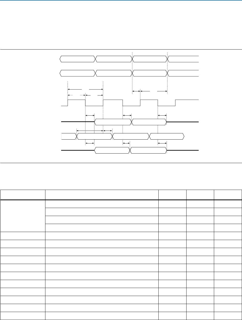
JSXZ
Update register valid output to high impedance — 25 ns
Notes to Table 3–41:
(1) Minimum clock period specified for 10 pF load on the
TDO
pin. Larger loads on
TDO
degrades the maximum
TCK
frequency.
(2) This specification is shown for 3.3-V LVTTL/LVCMOS and 2.5-V LVTTL/LVCMOS operation of the JTAG pins. For 1.8-V LVTTL/LVCMOS and
1.5-V LVCMOS operation, the t
JPSU
minimum is 6 ns and t
JPCO
, t
JPZX
, and t
JPXZ
are maximum values at 35 ns.
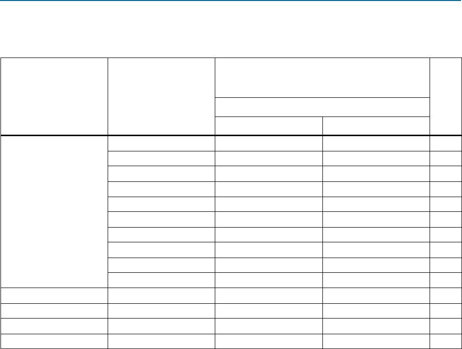
Table 3–41. JTAG Timing Parameters for MAX V Devices (Part 2 of 2)
Symbol Parameter Min Max Unit
Table 3–42. Document Revision History
Date Version Changes
May 2011 1.2 Updated Table 3–2, Table 3–15, Table 3–16, and Table 3–33.
January 2011 1.1 Updated Table 3–37, Table 3–38, Table 3–39, and Table 3–40.
December 2010 1.0 Initial release.