Nexperia
PESD2IVN24-T
ESD protection for In-vehicle networks
PESD2IVN24-T All information provided in this document is subject to legal disclaimers.
©
Nexperia B.V. 2018. All rights reserved
Product data sheet 1 February 2018 4 / 13
9. Characteristics
Table 6. Characteristics
Symbol Parameter Conditions Min Typ Max Unit
V
RWM
reverse standoff
voltage
T
amb
= 25 °C - - 24 V
V
BR
breakdown voltage I
R
= 10 mA; T
amb
= 25 °C [1] 25.5 30.5 35.5 V
I
RM
reverse leakage
current
V
RWM
= 24 V; T
amb
= 25 °C [1] - 1 50 nA
C
d
diode capacitance [1] - 14 17 pFf = 1 MHz; V
R
= 0 V; T
amb
= 25 °C
[2] - 0.1 - %ΔC
d
/C
d
diode capacitance
matching
f = 1 MHz; V
R
= 2.5 V; T
amb
= 25 °C [2] - 0.1 - %
I
PPM
= 1 A; t
p
= 8/20 µs; T
amb
= 25 °C [3] [1] - 31 40 V
I
PPM
= 3.5 A; t
p
= 8/20 µs; T
amb
= 25 °C [3] [1] - 33 42 V
V
CL
clamping voltage
I
PP
= 16 A; t
p
= TLP; T
amb
= 25 °C [4] [1] - 32 - V
R
dyn
dynamic resistance I
R
= 10 A; T
amb
= 25 °C [4] [1] - 0.2 - Ω
[1] Measured from pin 1 or 2 to pin 3.
[2] ∆C
d
is the difference of the capacitance measured between pin 1 and pin 3 and the capacitance measured between pin 2 and pin 3.
[3] Device stressed with 8/20 μs exponential decay waveform according to IEC 61000-4-5.
[4] Non-repetitive current pulse, Transmission Line Pulse (TLP); square pulse; ANSI / ESD STM5.5.1-2008
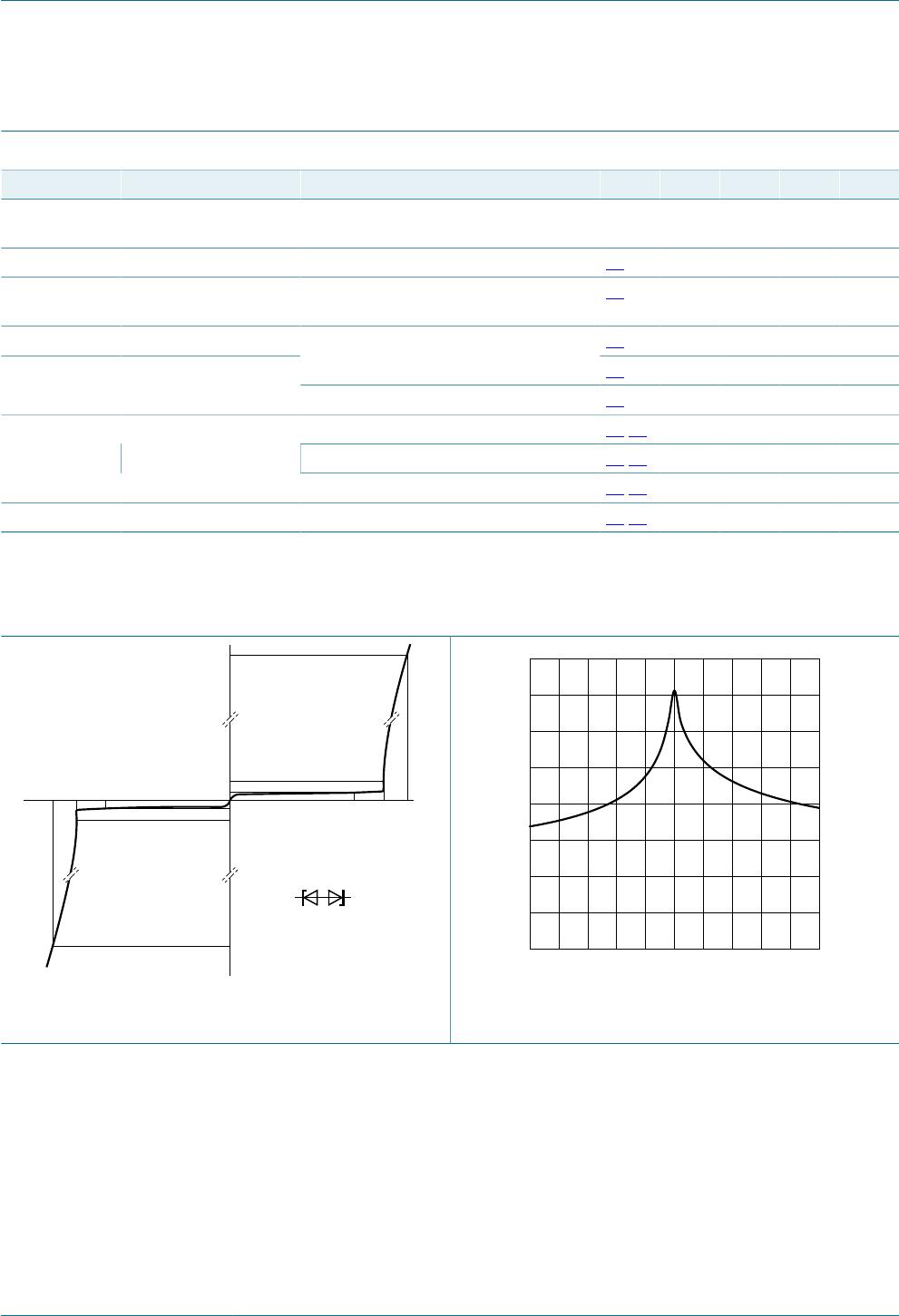
006aaa676
- V
CL
- V
BR
- V
RWM
V
CL
V
BR
V
RWM
- I
RM
I
RM
- I
R
I
R
- I
PP
I
PP
-
+
Fig. 3. V-I characteristics for a bidirectional ESD
protection diode
V
R
(V)
-25 255-5-15 15
aaa-027491
16
C
d
(pF)
0
2
4
6
8
10
12
14
Fig. 4. Diode capacitance as a function of reverse
voltage; typical values