LT3965/LT3965-1
15
39651fa
For more information www.linear.com/LT3965
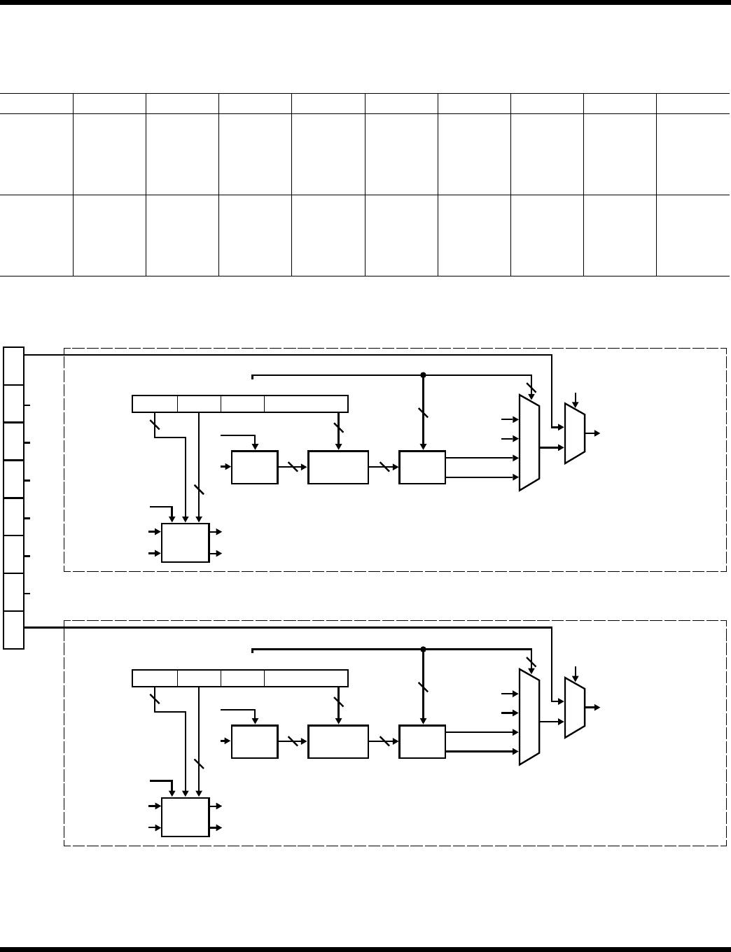
APPLICATIONS INFORMATION
Figure 6. LT3965/LT3965-1 I
2
C Serial Port ACMODE Write Protocol
Figure 7. LT3965/LT3965-1 I
2
C Serial Port ACMODE Read Protocol
condition. The repeated START (Sr) conditions are func-
tionally identical
to the START (S). Various combinations
of read/write commands are then possible within such
a transfer, except that the BCMODE write command for
dimming cycle synchronization and the BCMODE read com
-
mand for alert inquiry and the ACMODE write command
for
clearing the overheat fault bits must be self-contained
with a terminating STOP condition.
I
2
C SERIAL PORT DATA TRANSFER
After the START condition, the I
2
C bus is busy and data
transfer can begin between the master and the addressed
LT3965/LT3965-1 slave. Data is transferred over the bus in
group of nine bits, one byte followed by one acknowledge
(ACK) bit. The acknowledge signal is used for handshaking
between the master and the slave.
When the LT3965/LT3965-1 is written to, it acknowledges
its device write address and subsequent data bytes. The
data byte is transferred to an internal holding latch upon
the return of its acknowledge by the LT3965/LT3965-1.
If desired a repeated START (Sr) condition may be
initi-
ated by
the master to address another device on the I
2
C
bus for data transfer. The LT3965/LT3965-1 remembers
the valid data it has received. Once selected channels of
the devices on the I
2
C bus have been addressed and sent
valid data, the master issues a STOP condition to finish
the communication. The LT3965/LT3965-1 will update its
command registers with the data it has received upon the
STOP condition, except that the V
OTH
[1:0] and V
STH
[1:0]
bits are updated in the channel SCMREG command reg-
ister upon
the return of its acknowledge by the LT3965/
LT3965-1.
When
reading from the LT3965/LT3965-1, the LT3965/
LT3965-1 acknowledges its device read address and the
master acknowledges subsequent data bytes it has received
except the last one followed by a STOP or a repeated
START condition.
The master can free the I
2
C bus by issuing a STOP condi-
tion after the data transfer. If desired the master can verify
the
data bytes written to the internal holding latches prior
to updating them to the command registers by reading
them back before sending a STOP condition.
LT3965/LT3965-1 I
2
C COMMANDS AND WRITE/READ
PROTOCOLS
Only a master can issue an I
2
C command to start a write
or read operation. The first command byte is always an
I
2
C device address sent by a master. If the master issues
a write command, all the remaining bytes of the command
will be transmitted by the master. Otherwise, all the re
-
maining bytes of the command will be transmitted by the
addressed LT3965/LT3965-1 slave. The LT3965/LT3965-1
I
2
C commands can be divided into three categories based
on their purposes:
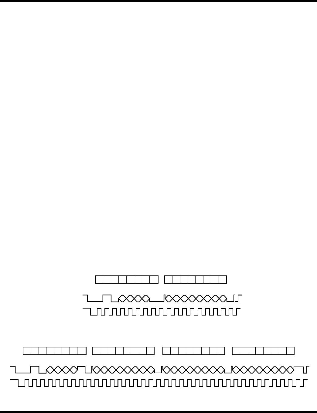
START STOP
SLAVE
ACK
SLAVE
ACK
0
0 1 0 A
4
A
3
ACMODE DEVICE ADDRESS DATA TO ACMREG
A
2
A
1
0(W)
1 2 3 4 5 6 7 8 9 1 2 3 4 5 6 7 8 9
3965 F06
0 0 SA SA1
SDA
SCL
B[7] B[6] B[5] B[4] B[3] B[2] B[1] B[0]
START STOP
SLAVE
ACK
MASTER
ACK
0
0 1 0 A
4
A
3
ACMODE DEVICE ADDRESS DATA FROM ACMREG
A
2
A
1
1(R)
1 2 3 4 5 6 7 8 9 1 2 3 4 5 6 7 8 9
1 2 3 4 5 6 7 8 9 1 2 3 4 5 6 7 8 9
3965 F07
0 1 SA MA
MASTER
ACK
MA
MASTER
NOT ACK
MNA1
SDA
SCL
B[7] B[6] B[5] B[4] B[3] B[2] B[1] B[0]
DATA FROM OLFREG
B[7] B[6] B[5] B[4] B[3] B[2] B[1] B[0]
DATA FROM SLFREG
B[7] B[6] B[5] B[4] B[3] B[2] B[1] B[0]