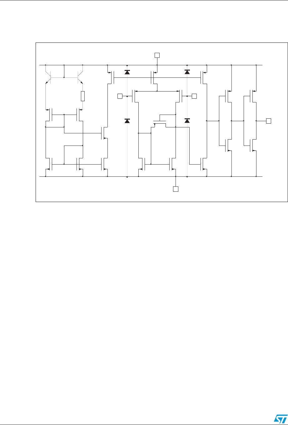
TS3704 Absolute maximum ratings
3/11
2 Absolute maximum ratings
Table 1. Absolute maximum ratings
Symbol Parameter Value Unit
V
CC
+
Supply voltage
(1)
1. All voltage values, except differential voltage, are with respect to network ground terminal.
18 V
V
id
Differential input voltage
(2)
2. Differential voltages are the non-inverting input terminal with respect to the inverting input terminal.
±18 V
V
i
Input voltage
(3)
3. The magnitude of the input and the output voltages must never exceed the magnitude of the positive and
negative supply voltages.
18 V
V
o
Output voltage 18 V
I
o
Output current 20 mA
I
F
Forward current in ESD protection diodes on input
(4)
4. Guaranteed by design.
50 mA
p
d
Power dissipation
(5)
DIP14
SO14
TSSOP14
5. Pd is calculated with T
amb
= +25°C, T
j
= +150°C and
R
thja
= 80°C/W for DIP14 package
R
thja
= 150°C/W for SO14 package
R
thja
= 175°C/W for TSSOP14 package
1500
830
710
mW
T
stg
Storage temperature range -65 to +150 °C
ESD
HBM: human body model
(6)
6. Human body model: A 100pF capacitor is charged to the specified voltage, then discharged through a
1.5kΩ resistor between two pins of the device. This is done for all couples of connected pin combinations
while the other pins are floating.
500 V
MM: machine model
(7)
7. Machine model: A 200pF capacitor is charged to the specified voltage, then discharged directly between
two pins of the device with no external series resistor (internal resistor < 5Ω). This is done for all couples of
connected pin combinations while the other pins are floating.
50 V
CDM: charged device model
(8)
8. Charged device model: all pins and the package are charged together to the specified voltage and then
discharged directly to the ground through only one pin. This is done for all pins.
1.5 kV
Table 2. Operating conditions
Symbol Parameter Value Unit
V
CC
+
Supply voltage
TS3704C, TS3704I
TS3704M
2.7 to 16
4 to 16
V
V
icm
Common mode input voltage range 0 to V
CC
+
-1.5 V
T
oper
Operating free-air temperature range
TS3704C
TS3704I
TS3704M
0 to +70
-40 to +125
-55 to +125
°C