NJM4560
-
-
Ver.2011-12-12
DUAL OPERATIONAL AMPLIFIER
■ GENERAL DESCRIPTION ■ PACKAGE OUTLINE
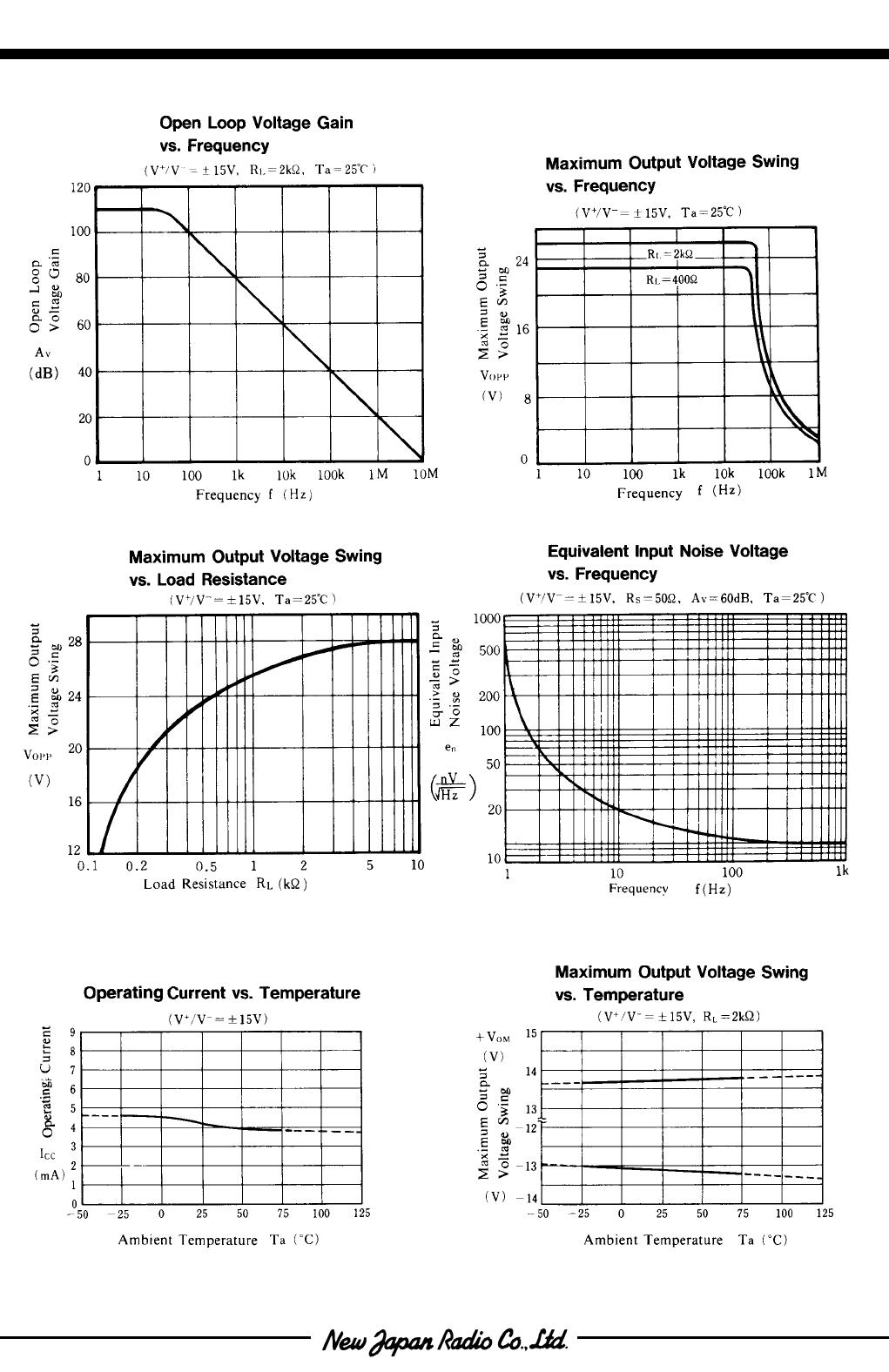
The NJM4560 integrated circuit is a high-gain, wide
bandwidth, dual operational amplifier capable of driving 20V
peak-to-peak into 400Ω loads. The NJM4560 combines
many of the features of the NJM4558 as well as providing the
capability of wider bandwidth, and higher slew rate make the
NJM4560 ideal for active filters, data and telecommunications,
and many instrumentation applications. The availability of the
NJM4560 in the surface mounted micro-package allows the
NJM4560 to be used in critical applications requiring very high
packing densities.
■ FEATURES
● Operating Voltage ( ±4V~±18V )
● Wide Gain Bandwidth Product ( 10MHz typ. )
● Slew Rate ( 4V/μs typ. )
● Package Outline DIP8, DMP8, SIP8, SOP8 JEDEC 150mil
● Bipolar Technology
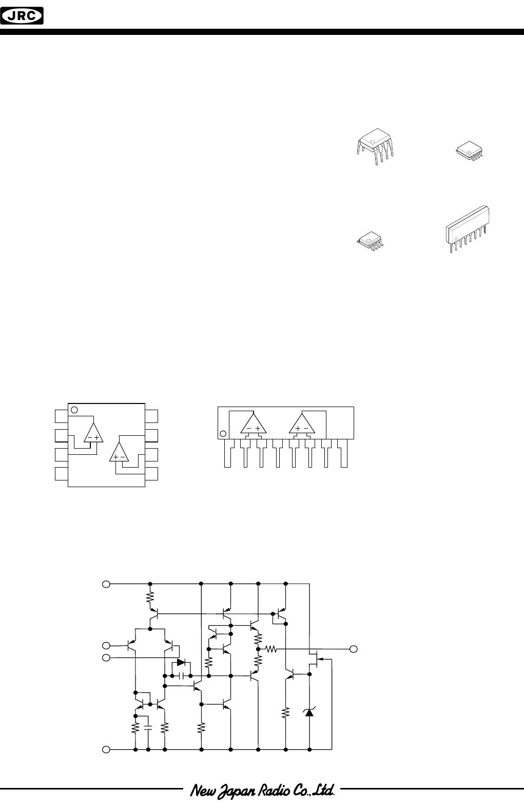
■ PIN CONFIGURATION
■ EQUIVALENT CIRCUIT ( 1/2 Shown )
NJM4560D
( DIP8)
NJM4560M
( DMP8 )
NJM4560E
( SOP8 )
NJM4560L
( SIP8 )
PIN FUNCTION
1. A OUTPUT
2. A - INPUT
3. A +INPUT
4. V
-
5. B +INPUT
6. B - INPUT
7. B OUTPUT
8. V
+
8
7
6
5
1
2
3
4
A
B
( Top View )
NJM4560D, NJM4560M, NJM4560E
A B
1 234567 8
NJM4560L
- INPUT
V
+
OUTPUT
+ INPUT
V
-