BAS21TM
Document number: DS35388 Rev. 5 - 2
1 of 4
www.diodes.com
February 2014
© Diodes Incorporated
BAS21TM
ADVANCE INFORMATION
SURFACE MOUNT HIGH VOLTAGE SWITCHING DIODE ARRAY
Features
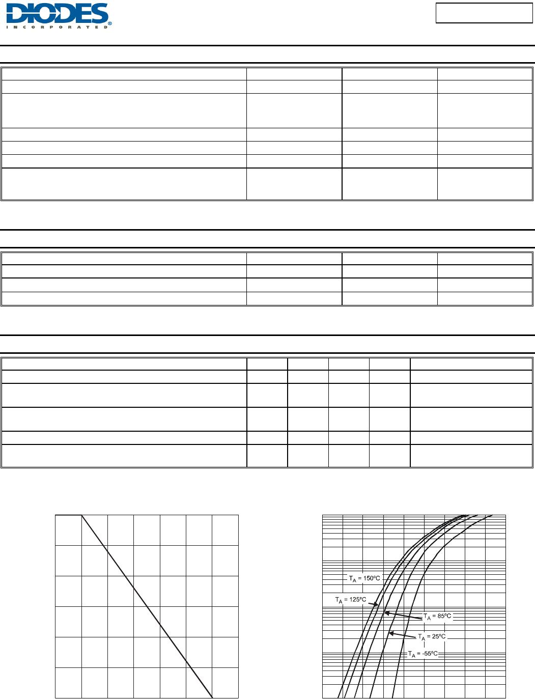
• Fast Switching Speed: max. 50ns
• Continuous Reverse Voltage: max. 200V
• Repetitive Peak Reverse Voltage: max. 250V
• Repetitive Peak Forward Current: max. 1A
• Small Surface Mount Package
• For General Purpose Switching Applications
• Totally Lead-Free & Fully RoHS Compliant (Notes 1 & 2)
• Halogen and Antimony Free. “Green” Device (Note 3)
• Qualified to AEC-Q101 Standards for High Reliability
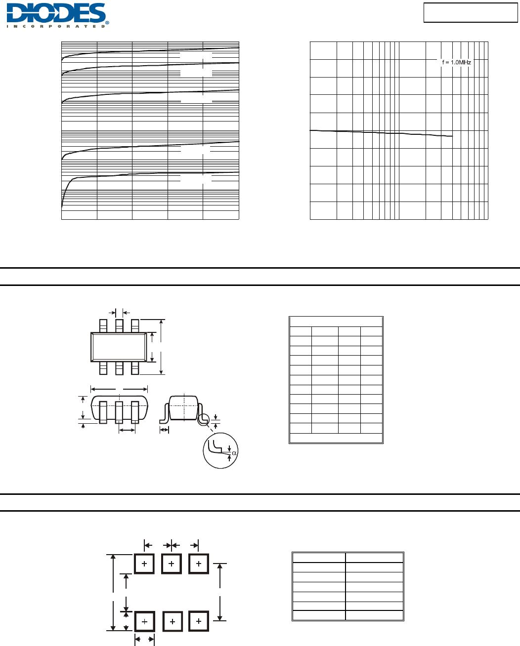
Mechanical Data
• Case: SOT26
• Case Material: Molded Plastic, "Green" Molding Compound,
UL Flammability Classification Rating 94V-0
• Moisture Sensitivity: Level 1 per J-STD-020
• Terminals: Matte Tin Finish annealed over Copper Alloy
leadframe (Lead Free Plating). Solderable per MIL-STD-202,
Method 208
• Orientation: See Diagram
• Weight: 0.009 grams (approximate)
Ordering Information (Notes 4)
Part Number Compliance Case Packaging
BAS21TM-7 AEC-Q101 SOT26 3,000/Tape & Reel
BAS21TMQ-13 Automotive SOT26 10,000/Tape & Reel
Notes: 1. No purposely added lead. Fully EU Directive 2002/95/EC (RoHS) & 2011/65/EU (RoHS 2) compliant.
2. See http://www.diodes.com/quality/lead_free.html for more information about Diodes Incorporated’s definitions of Halogen- and Antimony-free, "Green"
and Lead-free.
3. Halogen- and Antimony-free "Green” products are defined as those which contain <900ppm bromine, <900ppm chlorine (<1500ppm total Br + Cl) and
<1000ppm antimony compounds.
4. For packaging details, go to our website at http://www.diodes.com/products/packages.html.
Marking Information
Date Code Key
Year 2011 2012 2013 2014 2015 2016 2017 2018 2019 2020
Code Y Z A B C D E F G H
Month Jan Feb Mar Apr May Jun Jul Aug Sep Oct Nov Dec
Code 1 2 3 4 5 6 7 8 9 O N D
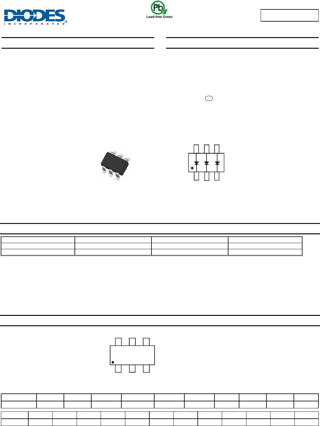
Top View
SOT26
Top View
Internal Schematic
XJJ = Product Type Marking Code
YM = Date Code Marking
Y =Year (ex: Z = 2012)
M = Month (ex: 9 = September)
XJJ
YM
e3