ZL30363GDG2

1
Copyright 2013, Microsemi Corporation. All Rights Reserved.
Features
Two independent clock channels
Frequency and Phase Sync over Packet Networks
Frequency accuracy performance for WCDMA-
FDD, GSM, LTE-FDD and femtocell applications
Frequency performance for ITU-T G.823 and
G.824 synchronization interface, as well as
G.8261 PNT PEC and CES interfaces
Phase Synchronization performance for
WCDMA-TDD, Mobile WiMAX, TD-SCDMA and
CDMA2000 applications
Client holdover and reference switching
between multiple Servers
Physical Layer Equipment Clocks Synchronization
ITU-T G.8262 for SyncE EEC option 1 and 2
ITU-T G.813 for SONET/SDH SEC option 1 and
2
Telcordia GR-1244 and GR-253 Stratum 3 and
SMC
Support for G.781 SETS
Any input clock rate from 1 Hz to 750 MHz
Automatic hitless reference switching and digital
holdover on reference fail
Flexible two-stage architecture to support
conversion between SONET/SDH and OTN rates
Digital PLLs with programmable bandwidth from
0.1 mHz up to 1 kHz
Programmable synthesizers
Any output clock rate from 1 Hz to 750 MHz
with maximum jitter below 0.63 ps RMS
Operates from a single crystal resonator or clock
oscillator
Configurable via SPI/I
2
C interface
May 2013
Figure 1 - Functional Block Diagram
Reference Monitors
State
Machine
Configuration
and Status
JTAG
Master Clock
ZL30363
Osci
Osco
Diff / Single Ended
Fr
0
= Br
0
*Kr
0
*Mr
0
/Nr
0
Ref0
JTAG
GPIO SPI / I
2
Cpwr_b
DPLL0/NCO0
Select Loop band.,
Phase slope limit
Ref1
Ref2
Ref3
Ref4
Ref5
Ref6
Ref7
Synthesizer 0
Fs= Bs
0
*Ks
0
*16*Ms
0
/Ns
0
LVPECL
LVCMOS
Div A
LVPECL
LVCMOS
Clock Generator 0
Div B
Div C
Div D
Synthesizer 1
Fs= Bs
1
*Ks
1
*16*Ms
1
/Ns
1
LVPECL
LVCMOS
Div A
LVPECL
LVCMOS
Clock Generator 1
Div B
Div C
Div D
Synthesizer 2
Fs= Bs
2
*Ks
2
*16*Ms
2
/Ns
2
LVPECL
LVCMOS
Div A
LVPECL
LVCMOS
Clock Generator 2
Div B
Div C
Div D
Synthesizer 3
Fs= Bs
3
*Ks
3
*16*Ms
3
/Ns
3
LVPECL
LVCMOS
Div A
LVPECL
LVCMOS
Clock Generator 3
Div B
Div C
Div D
Diff / Single Ended
Fr
1
= Br
1
*Kr
1
*Mr
1
/Nr
1
Diff / Single Ended
Fr
2
= Br
2
*Kr
2
*Mr
2
/Nr
2
Diff / Single Ended
Fr
3
= Br
3
*Kr
3
*Mr
3
/Nr
3
Diff / Single Ended
Fr
4
= Br
4
*Kr
4
*Mr
4
/Nr
4
Diff / Single Ended
Fr
5
= Br
5
*Kr
5
*Mr
5
/Nr
5
Diff / Single Ended
Fr
6
= Br
6
*Kr
6
*Mr
6
/Nr
6
Diff / Single Ended
Fr
7
= Br
7
*Kr
7
*Mr
7
/Nr
7
DPLL1/NCO1
Select Loop band.,
Phase slope limit
hpdiff1_p/n
hpoutclk0
hpdiff0_p/n
hpoutclk1
hpdiff3_p/n
hpoutclk2
hpdiff2_p/n
hpoutclk3
hpdiff5_p/n
hpoutclk4
hpdiff4_p/n
hpoutclk5
hpdiff7_p/n
hpoutclk6
hpdiff6_p/n
hpoutclk7
Single Ended
Fr
9
= Br
9
*Kr
9
*Mr
9
/Nr
9
Single Ended
Fr
10
= Br
10
*Kr
10
*Mr
10
/Nr
10
Ref9
Ref10
Ref8
Diff / Single Ended
Fr
8
= Br
8
*Kr
8
*Mr
8
/Nr
8
ZL30363
IEEE 1588 and Synchronous Ethernet Packet
Clock Network Synchronizer
Short Form Data Sheet
Ordering Information:
ZL30363GDG2 144 Pin LBGA
Trays
Pb Free Tin/Silver/Copper
-40
o
C to +85
o
C
Package size: 13 x 13 mm
ZL30363 Short Form Data Sheet
2
Microsemi Corporation
Detailed Features
General
Two independent clock channels
Operates from a single crystal resonator or clock oscillator
Configurable via its SPI/I
2
C interface
Time Synchronization Algorithm
External algorithm controls software digital PLL to adjust frequency and phase alignment
Frequency, Phase and Time Synchronization over IP, MPLS and Ethernet Packet Networks
Frequency accuracy performance for WCDMA-FDD, GSM, LTE-FDD and femtocell applications, with target
performance less than ± 15 ppb.
Frequency performance for ITU-T G.823 and G.824 synchronization interface, as well as G.8261 PNT EEC,
PNT PEC and CES interface specifications.
Phase Synchronization performance for WCDMA-TDD, Mobile WiMAX, TD-SCDMA and CDMA2000
applications with target performance less than ± 1 s phase alignment.
Time Synchronization for UTC-traceability and GPS replacement.
Client reference switching between multiple Servers
Client holdover when Server packet connectivity is lost
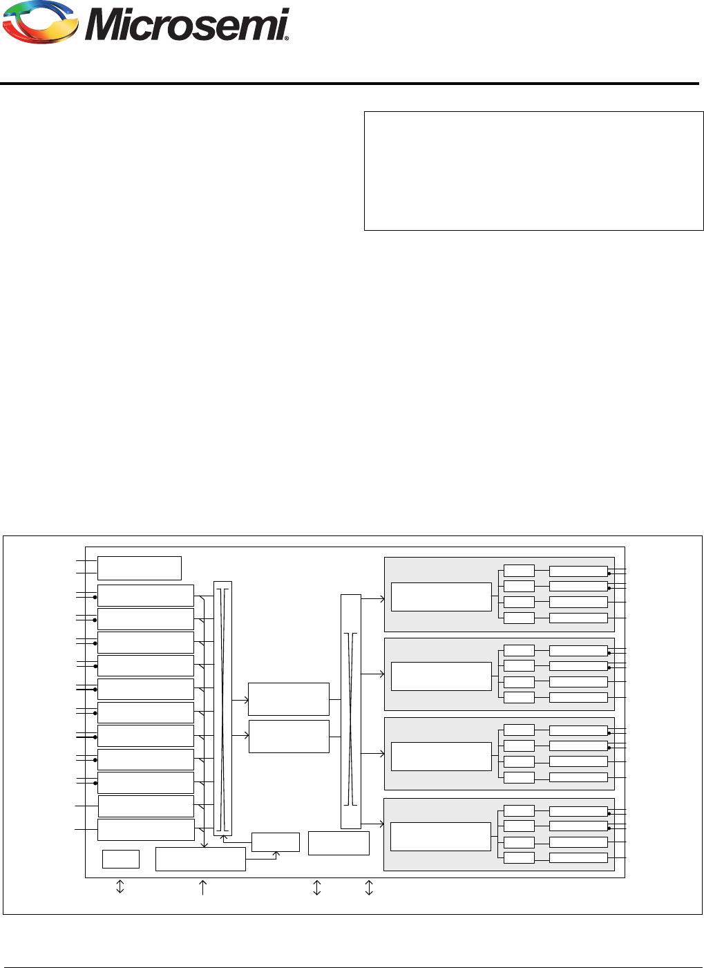
Electrical Clock Inputs
Nine input references configurable as single ended or differential and two single ended input references
Synchronize to any clock rate from 1 Hz to 750 MHz on differential inputs
Synchronize to any clock rate from 1 Hz to 177.75 MHz on singled-ended inputs
Any input reference can be fed with sync (frame pulse) or clock.
Synchronize to sync pulse and sync pulse/clock pair.
Flexible input reference monitoring automatically disqualifies references based on frequency and phase
irregularities
•LOS
Single cycle monitor
Precise frequency monitor
Coarse frequency monitor
Guard soak timer
Per input clock delay compensation
Electrical Clock Engine
Digital PLLs filter jitter from 0.1 mHz up to 1 kHz
Flexible two-stage architecture translates between arbitrary data rates, line coding rates and FEC rates
Internal state machine automatically controls mode of operation (free-run, locked, holdover)
Automatic hitless reference switching and digital holdover on reference fail
Physical-to-physical reference switching
ZL30363 Short Form Data Sheet
3
Microsemi Corporation
Physical-to-packet reference switching
Packet-to-physical reference switching
Packet-to-packet reference switching
Support for wide variety of Equipment Clock specifications
SyncE
ITU-T G.8262 option 1 EEC (Europe/China)
ITU-T G.8262 option 2 (USA)
•SONET/SDH
ITU-T G.813 option 1 SEC (Europe/China)
ITU-T G.813 option 2 (USA)
ANSI T1.105/Telcordia GR-253 Stratum 3 for SONET
Telcordia GR-253 SMC
•PDH
ITU-T G.812 Type I SSU
ITU-T G.812 Type III, ANSI T1.101/Telcordia GR-1244 Stratum 3E, including phase build out
ANSI T1.101/Telcordia GR-1244 Stratum 3
ANSI T1.101/Telcordia GR-1244 Stratum 4E/4
Selectable phase slope limiting
Holdover better than 1 ppb (when using < 0.1 Hz filter)
Supports ITU-T G.823, G.824 and G.8261 for 2048 kbit/s and 1544 kbit/s interfaces
Supports G.781 SETS
Electrical Clock Generation
Four programmable synthesizers
Eight LVPECL outputs
Two LVPECL outputs per synthesizer
Generate any clock rate from 1 Hz to 750 MHz
Maximum jitter below 0.63 ps rms
Meets OC-192, STM-64, 1 GbE and 10 GbE interface jitter requirements
Eight LVCMOS outputs
Two LVCMOS outputs per synthesizer
Generate any clock rate from 1 Hz to 177.75 MHz
Programmable output advancement/delay to accommodate trace delays or compensate for system routing
paths
Outputs may be disabled to save power
API Software
Interfaces to 1588-capable PHY and switches with integrated timestamping
Abstraction layer for independence from OS and CPU, from embedded SoC to home-grown
Fits into centralized, highly integrated pizza box architectures as well as distributed architectures with
multiple line cards and timing cards

ZL30363GDG2

Mfr. #:
Manufacturer:
Microchip / Microsemi
Description:
Clock Generators & Support Products
Lifecycle:
New from this manufacturer.
Delivery:
DHL FedEx Ups TNT EMS
Payment:
T/T Paypal Visa MoneyGram Western Union

Products related to this Datasheet