2
10
-2
10
-3
10
-4
10
-5
10
-6
10
-7
10
-8
10
-9
10
-10
10
-11
10
-12
10
-13
10
-14
10
-15
-5
LINEAR EXTRAPOLATION OF
10
-4
THROUGH 10
-7
DATA
ACTUAL DATA
-4 -3 -2
-1
0
1
3
BIT ERROR RATIO
2
Applications Information
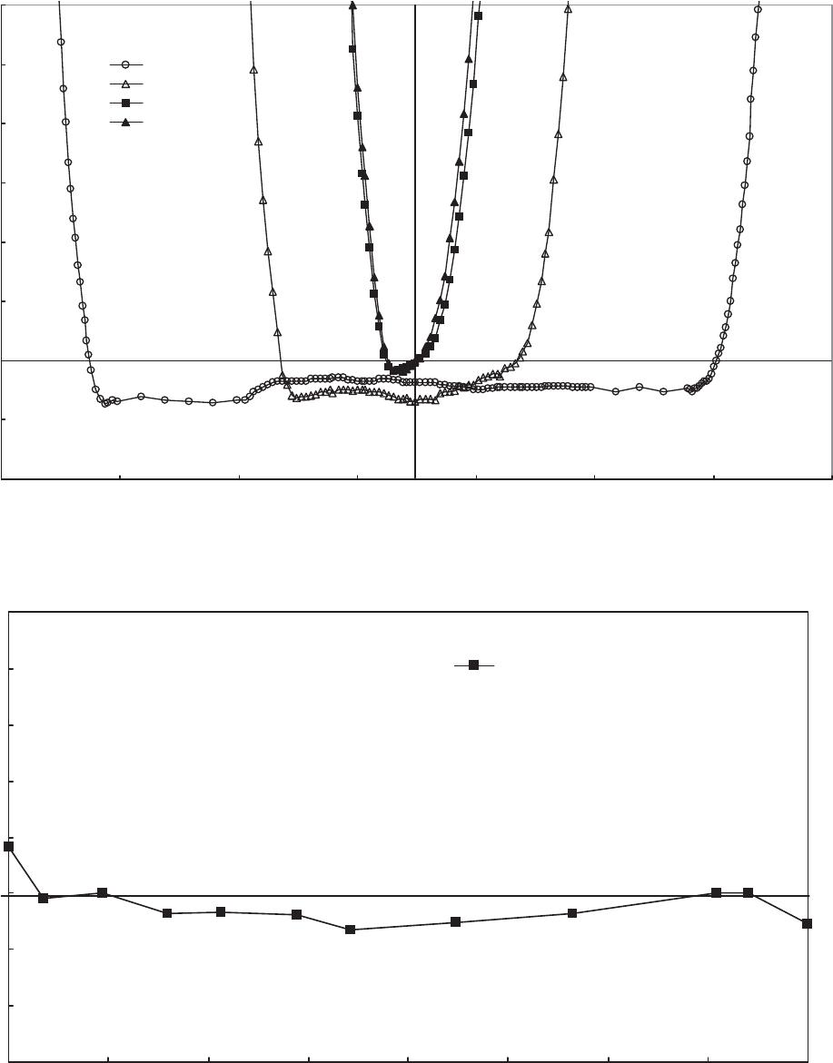
Typical BER Performance of HFBR-5208xxxZ Receiver versus Input Optical Power Level
Relative Input Optical Power amount (dB) is referenced to
the absolute level (dBm avg.) given in the Receiver Optical
Characteristics table. The 0 ns sampling time position
for this Figure 2 refers to the center of the Baud interval
for the particular signaling rate. The Baud interval is the
reciprocal of the signaling rate in MBd. For example, at
622 MBd the Baud interval is 1.61 ns, at 155 MBd the Baud
interval is 6.45 ns. Test conditions for this tub diagram are
listed in Figure 2.
The HFBR-5208xxxZ receiver input optical power require-
ments vary slightly over the signaling rate range of 20
MBd to 700 MBd for a constant bit-error-ratio (BER) of
10
-10
condition. Figure 3 illustrates the typical receiver
relative input optical power varies by <0.7 dB over this
full range. This small sensitivity variation allows the
optical budget to remain nearly constant for designs that
make use of the broad signaling rate range of the HFBR-
5208xxxZ. The curve has been normalized to the input
optical power level (dBm avg.) of the receiver for 622 MBd
at center of the Baud interval with a BER of 10
-10
. The data
patterns that can be used at these signaling rates should
be, on average, balanced duty factor of 50%. Momentary
excursions of less or more data duty factor than 50% can
occur, but the overall data pattern must remain balanced.
Unbalanced data duty factor will cause excessive pulse-
width distortion, or worse, bit errors. The test conditions
are listed in Figure 3.
Recommended Circuit Schematic
When designing the HFBR-5208xxxZ circuit interface, there
are a few fundamental guidelines to follow. For example, in
the Recommended Circuit Schematic, Figure 4, the di erential
data lines should be treated as 50 ohm Microstrip or stripline
transmission lines. This will help to minimize the parasitic
inductance and capacitance e ects. Proper termination of
the di erential data signal will prevent re ections and ringing
which would compromise the signal delity and generate
unwanted electrical noise. Locate termination at the received
signal end of the transmission line. The length of these lines
should be kept short and of equal length to prevent pulse-
width distortion from occurring. For the high-speed signal
lines, di erential signals should be used, not single-ended
signals. These di erential signals need to be loaded symmetri-
cally to prevent unbalanced currents from owing which will
cause distortion in the signal.
Figure 1. Relative Input Optical Power - dBm Average.
The HFBR-5208xxxZ transceiver can be operated at Bit-
Error-Ratio conditions other than the required BER = 1
x 10
-10
of the 622 MBd ATM Forum 622.08 Mb/s Physical
Layer Standard and the ANSI T1.646a. The typical trade-
o of BER versus Relative Input Optical Power is shown
in Figure 1. The Relative Input Optical Power in dB is
referenced to the Input Optical Power parameter value
in the Receiver Optical Characteristics table. For better
BER condition than 1 x 10
-10
, more input signal is needed
(+dB). For example, to operate the HFBR-5208xxxZ at a
BER of 1 x 10
-12
, the receiver will require an input signal
approximately 0.6 dB higher than the -26 dBm level re-
quired for 1 x 10
-10
operation, i.e. -25.4 dBm.
An informative graph of a typical, short ber transceiver
link per-formance can be seen in Figure 2. This gure is
useful for designing short reach links with time-based
jitter requirements. This gure indicates Relative Input
Optical Power versus Sampling Time Position within the
receiver output data eye-opening. The given curves are
at a constant bit-error-ratio (BER) of 10
-10
for four di er-
ent signaling rates, 155 MBd, 311 MBd, 622 MBd and 650
MBd. These curves, called “tub” diagrams for their shape,
show the amount of data eye-opening time-width for
various receiver input optical power levels. A wider data
eye-opening provides more time for the clock recovery
circuit to operate within without creating errors. The
deeper the tub is indicates less input optical power is
needed to operate the receiver at the same BER condition.
Generally, the wider and deeper the tub is the better. The