4
MOUNTING POST
NO INTERNAL CONNECTION
HFBR-5208xxxZ
TOP VIEW
V
EER
RD RD SD V
CCR
V
CCT
TD TD V
EET
123456789
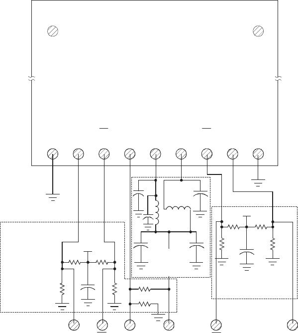
C2
L1 L2
R2 R3
R1 R4
C5
C3 C4
R9
R10
V
CC
FILTER
AT V
CC
PINS
TRANSCEIVER
R5 R7
R6 R8
C6
RD RD SD V
CC
TD TD
TERMINATION
AT PHY
DEVICE
INPUTS
TERMINATION
AT TRANSCEIVER
INPUTS
Rx Rx Tx Tx
V
CC
V
CC
C1
C7
MOUNTING POST
NO INTERNAL CONNECTION
NOTES:
THE SPLIT-LOAD TERMINATIONS FOR PECL SIGNALS
NEED TO BE LOCATED AT THE INPUT OF DEVICES
RECEIVING THOSE PECL SIGNALS. RECOMMEND
MULTI-LAYER PRINTED CIRCUIT BOARD WITH 50 OHM
MICROSTRIP OR STRIPLINE SIGNAL PATHS BE USED.
R1 = R4 = R6 = R8 = R10 = 130 OHMS.
R2 = R3 = R5 = R7 = R9 = 82 OHMS.
C1 = C2 = C3 = C5 = C6 = 0.1 F.
C4 = C7 = 10 F.
L1 = L2 = 1 H COIL OR FERRITE INDUCTOR
(see text comments).
Maintain a solid, low inductance ground plane for returning
signal currents to the power supply. Multilayer plane printed
circuit board is best for distribution of V
CC
, returning ground
currents, forming transmission lines and shielding. Also, it
is important to suppress noise from in uencing the ber-
optic transceiver per-formance, especially the receiver
circuit. Proper power supply ltering of V
CC
for this trans-
ceiver is accomplished by using the recommended sepa-
rate lter circuits shown in Figure 4. These lter circuits
suppress V
CC
noise of 100 mV peak-to-peak or less over
a broad frequency range. This prevents receiver sensitiv-
ity degradation . It is recommended that surface-mount
components be used. Use tantalum capacitors for the 10
μF capacitors and monolithic, ceramic bypass capacitors
for the 0.1 μF capacitors. Also, it is recommended that a
surface-mount coil inductor of 1 μH be used. Ferrite beads
can be used to replace the coil inductors when using
quieter V
CC
supplies, but a coil inductor is recom mended
over a ferrite bead to provide low-frequency noise ltering
as well. Coils with a low, series dc resistance (<0.7 ohms)
Figure 4. Recommended Circuit Schematic for dc Coupling (at +5 V) between Optical Transceiver and Physical Layer IC
and high, self-resonating frequency are recommended. All
power supply components need to be placed physically
next to the V
CC
pins of the receiver and transmitter. Use a
good, uniform ground plane with a minimum number of
holes to provide a low-inductance ground current return
path for the signal and power supply currents.
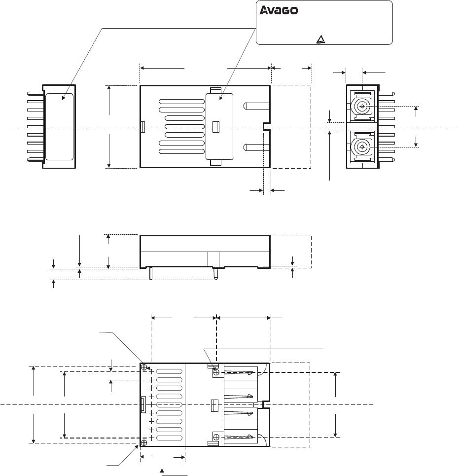
Although the front mounting posts make contact with the
metallized housing, these posts should not be relied upon to
provide adequate electrical connection to the plated housing.
It is recommended to either connect these front posts to
chassis ground or allow them to remain unconnected. These
front posts should not be connected to signal ground.
Figure 5 shows the recommended board layout pattern.
In addition to these recommendations, Avago Technologies
Application Engineering sta is available for consulting
on best layout practices with various vendors’ serializer/
deserializer, clock recovery/generation integrated circuits.