LT6660HCDC-5#TRPBF

LT6660
1
6660fa
CHANGE IN V
OUT
(%)
–0.09
0
DISTRIBUTION (%)
4
8
16
20
24
32
6660 TA01b
12
28
0.09
–0.05
0.01–0.01 0.05
Tiny Micropower
Precision Series References
in 2mm × 2mm DFN
The LT
®
6660 is a family of micropower series references
that combine high accuracy and low drift with low power
dissipation and extremely small package size. These se-
ries references use curvature compensation to obtain
low temperature coefficient, and laser trimmed precision
thin-film resistors to achieve high output accuracy. The
LT6660 will supply up to 20mA with excellent line regula-
tion characteristics, making it ideal for precision regulator
applications.
The LT6660 family of series references provide supply
current and power dissipation advantages over shunt
references that must idle the entire load current to oper-
ate. Additionally, the LT6660 does not require an output
compensation capacitor. This feature is important in
applications where PC board space is a premium, fast set-
tling is demanded, or total capacitance must be kept to a
minimum, as in intrinsic safety applications. Reverse-bat-
tery protection keeps these references from conducting
reverse current.
Handheld Instruments
Precision Regulators
A/D and D/A Converters
Power Supplies
Hard Disk Drives
Sensor Modules
No Output Capacitor Required
Low Drift: 20ppm/°C Max
High Accuracy: 0.2% Max
Low Supply Current
20mA Output Current Guaranteed
Reverse-Battery Protection
Low IR Reflow Induced Stress: 0.02% Typ
Voltage Options: 2.5V, 3V, 3.3V, 5V and 10V
Space-Saving Alternative to the LT1460
3-Lead 2mm × 2mm × 0.75mm DFN Package
APPLICATIO S
U
FEATURES
DESCRIPTIO
U
TYPICAL APPLICATIO
U
, LT, LTC and LTM are registered trademarks of Linear Technology Corporation.
All other trademarks are the property of their respective owners.
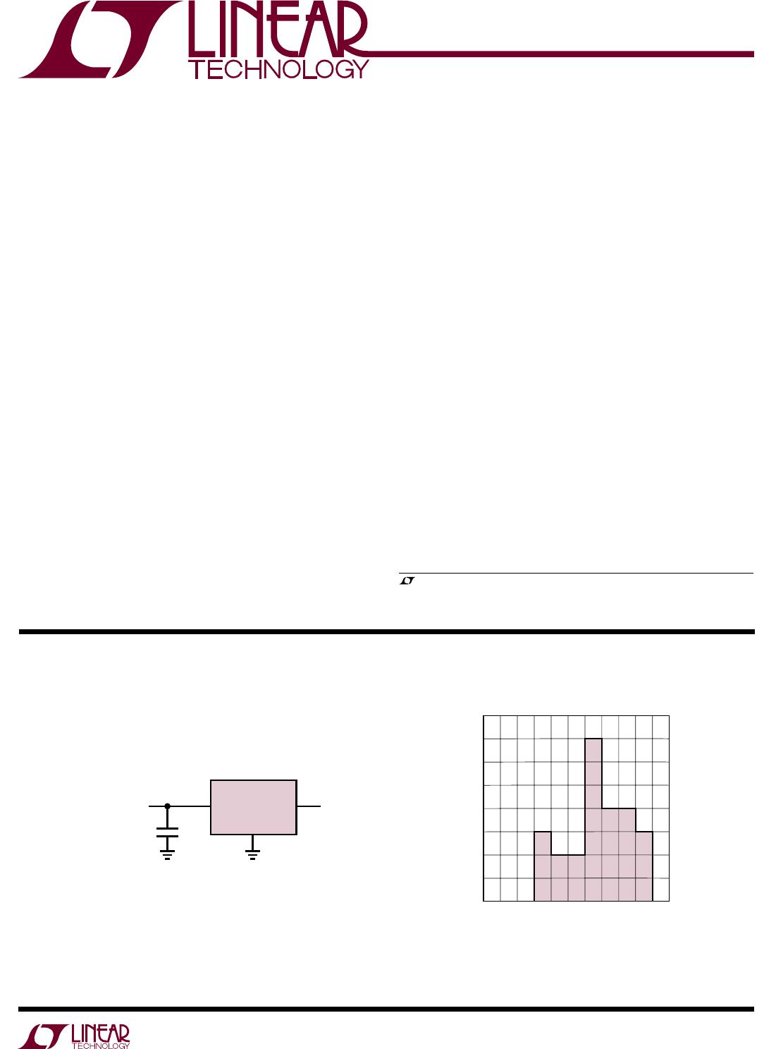
Basic Connection
LT6660
GND
IN
OUT
V
OUT
+ 0.9V V
IN
20V
6660 TA01
C1
0.1µF
V
OUT
LT6660H V
OUT
Shift Due to IR Reflow
LT6660
2
6660fa
Input Voltage .............................................................30V
Reverse Voltage ......................................................–15V
Output Short-Circuit Duration, T
A
= 25°C ................5 sec
Specified Temperature Range ...................... 0°C to 70°C
(Note 1)
PACKAGE/ORDER I FOR ATIO
U UW
TOP VIEW
OUT
GND
IN
DC PACKAGE
3-LEAD (2mm × 2mm) PLASTIC DFN
4
3
2
1
T
JMAX
= 125°C, θ
JA
= 102°C/W
EXPOSED PAD IS GND, MUST BE SOLDERED TO PCB
ORDER PART NUMBER DFN PART MARKING*
LT6660HCDC-2.5
LT6660JCDC-2.5
LT6660KCDC-2.5
LT6660HCDC-3
LT6660JCDC-3
LT6660KCDC-3
LT6660HCDC-3.3
LT6660JCDC-3.3
LT6660KCDC-3.3
LT6660HCDC-5
LT6660JCDC-5
LT6660KCDC-5
LT6660HCDC-10
LT6660JCDC-10
LT6660KCDC-10
LBXN
LBXN
LBXN
LBYV
LBYV
LBYV
LBYW
LBYW
LBYW
LBYT
LBYT
LBYT
LBYX
LBYX
LBYX
Order Options Tape and Reel: Add #TR
Lead Free: Add #PBF Lead Free Tape and Reel: Add #TRPBF
Lead Free Part Marking: http://www.linear.com/leadfree/
Consult LTC Marketing for parts specified with wider operating temperature ranges. *The temperature grade is identified by a label on the shipping container.
Operating Temperature Range
(Note 2) ............................................... –40°C to 85°C
Storage Temperature Range (Note 3) ..... –65°C to 150°C
Lead Temperature (Soldering, 10 sec) .................. 300°C
AVAILABLE OPTIONS
OUTPUT VOLTAGE
(V)
SPECIFIED TEMPERATURE
RANGE
ACCURACY
(%)
TEMPERATURE
COEFFICIENT (ppm/°C)
PART ORDER
NUMBER
2.5
2.5
2.5
0°C to 70°C
0°C to 70°C
0°C to 70°C
0.2
0.4
0.5
20
20
50
LT6660HCDC-2.5
LT6660JCDC-2.5
LT6660KCDC-2.5
3
3
3
0°C to 70°C
0°C to 70°C
0°C to 70°C
0.2
0.4
0.5
20
20
50
LT6660HCDC-3
LT6660JCDC-3
LT6660KCDC-3
3.3
3.3
3.3
0°C to 70°C
0°C to 70°C
0°C to 70°C
0.2
0.4
0.5
20
20
50
LT6660HCDC-3.3
LT6660JCDC-3.3
LT6660KCDC-3.3
LT6660
3
6660fa
The denotes the specifications which apply over the full operating
temperature range, otherwise specifications are at T
A
= 25°C. V
IN
= V
OUT
+ 2.5V, I
OUT
= 0 unless otherwise specified.
ELECTRICAL CHARACTERISTICS
OUTPUT VOLTAGE
(V)
SPECIFIED TEMPERATURE
RANGE
ACCURACY
(%)
TEMPERATURE
COEFFICIENT (ppm/°C)
PART ORDER
NUMBER
5
5
5
0°C to 70°C
0°C to 70°C
0°C to 70°C
0.2
0.4
0.5
20
20
50
LT6660HCDC-5
LT6660JCDC-5
LT6660KCDC-5
10
10
10
0°C to 70°C
0°C to 70°C
0°C to 70°C
0.2
0.4
0.5
20
20
50
LT6660HCDC-10
LT6660JCDC-10
LT6660KCDC-10
AVAILABLE OPTIONS
PARAMETER CONDITIONS MIN TYP MAX UNITS
Output Voltage Tolerance LT6660HCDC –0.2 0.2 %
LT6660JCDC –0.4 0.4 %
LT6660KCDC –0.5 0.5 %
Output Voltage Temperature Coefficient (Note 4) LT6660HCDC
LT6660JCDC
LT6660KCDC
10
10
25
20
20
50
ppm/°C
ppm/°C
ppm/°C
Line Regulation V
OUT
+ 0.9V ≤ V
IN
≤ V
OUT
+ 2.5V
150 800
1000
ppm/V
ppm/V
V
OUT
+ 2.5V ≤ V
IN
≤ 20V
50 100
130
ppm/V
ppm/V
Load Regulation Sourcing (Note 5) I
OUT
= 100µA
1000 3000
4000
ppm/mA
ppm/mA
I
OUT
= 10mA
50 200
300
ppm/mA
ppm/mA
I
OUT
= 20mA
20 70
100
ppm/mA
ppm/mA
Thermal Regulation (Note 6) ΔP = 200mW 2.5 10 ppm/mW
Dropout Voltage (Note 7) V
IN
– V
OUT
, ΔV
OUT
≤ 0.2%, I
OUT
= 0
0.9 V
V
IN
– V
OUT
, ΔV
OUT
≤ 0.2%, I
OUT
= 10mA
1.3
1.4
V
V
Output Current Short V
OUT
to GND 40 mA
Reverse Leakage V
IN
= –15V
0.5 10 µA
Output Voltage Noise (Note 8) 0.1Hz ≤ f ≤ 10Hz
10Hz ≤ f ≤ 1kHz
4
4
ppm (P-P)
ppm (RMS)
Long-Term Stability of Output Voltage (Note 9) 100 ppm/√kHr
Hysteresis (Note 10) ΔT = 0°C to 70°C
ΔT = –40°C to 85°C
50
250
ppm
ppm
Supply Current LT6660-2.5
115 145
175
µA
µA
LT6660-3
145 180
220
µA
µA
LT6660-3.3
145 180
220
µA
µA
LT6660-5
160 200
240
µA
µA
LT6660-10
215 270
350
µA
µA

LT6660HCDC-5#TRPBF

Mfr. #:
Manufacturer:
Analog Devices Inc.
Description:
Voltage References 5V Low Cost uP Prec Series Ref.
Lifecycle:
New from this manufacturer.
Delivery:
DHL FedEx Ups TNT EMS
Payment:
T/T Paypal Visa MoneyGram Western Union