OP295/OP495
Rev. G | Page 10 of 16
Finally, the potentiometer, R8, is needed to adjust the offset
voltage to null it to zero. Similar performance can be obtained
using an OP90 as the output amplifier with a savings of about
185 A of supply current. However, the output swing does not
include the positive rail, and the bandwidth reduces to approxi-
mately 250 Hz.
Table 6. Single-Supply Low Noise Preamp Performance
I
C
= 1.85 mA I
C
= 0.5 mA
R1 270 Ω 1.0 kΩ
R3, R4 200 Ω 910 Ω
e
n
@ 100 Hz 3.15 nV/√Hz 8.6 nV/√Hz
e
n
@ 10 Hz 4.2 nV/√Hz 10.2 nV/√Hz
I
SY
4.0 mA 1.3 mA
I
B
11 A 3 µA
Bandwidth 1 kHz 1 kHz
Closed-Loop Gain 1000 1000
DRIVING HEAVY LOADS
The OP295/OP495 are well suited to drive loads by using a
power transistor, Darlington, or FET to increase the current to
the load. The ability to swing to either rail can assure that the
device is turned on hard. This results in more power to the load
and an increase in efficiency over using standard op amps with
their limited output swing. Driving power FETs is also possible
with the OP295/OP495 because of their ability to drive capaci-
tive loads of several hundred picofarads without oscillating.
Without the addition of external transistors, the OP295/OP495
can drive loads in excess of ±15 mA with ±15 V or +30 V
supplies. This drive capability is somewhat decreased at lower
supply voltages. At ±5 V supplies, the drive current is ±11 mA.
Driving motors or actuators in two directions in a single-supply
application is often accomplished using an H bridge. The
principle is demonstrated in Figure 21. From a single 5 V
supply, this driver is capable of driving loads from 0.8 V to
4.2 V in both directions. Figure 22 shows the voltages at the
inverting and noninverting outputs of the driver. There is a
small crossover glitch that is frequency-dependent; it does not
cause problems unless used in low distortion applications, such
as audio. If this is used to drive inductive loads, diode clamps
should be added to protect the bridge from inductive kickback.
10k
1.67V
2N2222 2N2222
OUTPUTS
2N2907
2N2907
5
V
10k 10k
0 V
IN
2.5V
5k
+
+
00331-019
Figure 21. H Bridge
10
90
100
0%
2V
2V
1ms
00331-020
Figure 22. H Bridge Outputs
DIRECT ACCESS ARRANGEMENT
The OP295/OP495 can be used in a single-supply direct access
arrangement (DAA), as shown in Figure 23. This figure shows
a portion of a typical DM capable of operating from a single 5 V
supply, and it may also work on 3 V supplies with minor modi-
fications. Amplifier A2 and Amplifier A3 are configured so that
the transmit signal, TxA, is inverted by A2 and is not inverted
by A3. This arrangement drives the transformer differentially so
the drive to the transformer is effectively doubled over a single
amplifier arrangement. This application takes advantage of the
ability of the OP295/OP495 to drive capacitive loads and to save
power in single-supply applications.
+
+
2.5V REF
A3
750pF
A1
37.4k
390pF
RxA
TxA
A2
3.3k
20k
475
22.1k
20k
20k
20k
20k
0.033µF
1:1
+
0.0047µF
OP295/
OP495
OP295/
OP495
OP295/
OP495
0.1µF
0.1µF
00331-021
Figure 23. Direct Access Arrangement
SINGLE-SUPPLY INSTRUMENTATION AMPLIFIER
The OP295/OP495 can be configured as a single-supply
instrumentation amplifier, as shown in Figure 24. For this
example, V
REF
is set equal to V+/2, and V
O
is measured with
respect to V
REF
. The input common-mode voltage range
includes ground, and the output swings to both rails.
OP295/OP495
Rev. G | Page 11 of 16
V+
+
+
5
3
2
1
6
8
4
7
1
/
2
OP295/
OP495
1/2
OP295/
OP495
+
V
IN
V
O
R4
100k
R3
20k
R2
20k
R1
100k
V
REF
R
G
V
O
=
(
5+
200k
)
V
IN
+V
REF
R
G
00331-022
Figure 24. Single-Supply Instrumentation Amplifier
Resistor R
G
sets the gain of the instrumentation amplifier.
Minimum gain is 6 (with no R
G
). All resistors should be matched
in absolute value as well as temperature coefficient to maximize
common-mode rejection performance and minimize drift. This
instrumentation amplifier can operate from a supply voltage as
low as 3 V.
SINGLE-SUPPLY RTD THERMOMETER AMPLIFIER
This RTD amplifier takes advantage of the rail-to-rail swing of
the OP295/OP495 to achieve a high bridge voltage in spite of a
low 5 V supply. The OP295/OP495 amplifier servos a constant
200 A current to the bridge. The return current drops across
the parallel resistors 6.19 kΩ and 2.55 M, developing a voltage
that is servoed to 1.235 V, which is established by the AD589
band gap reference. The 3-wire RTD provides an equal line
resistance drop in both 100  legs of the bridge, thus improving
the accuracy.
The AMP04 amplifies the differential bridge signal and converts
it to a single-ended output. The gain is set by the series resis-
tance of the 332  resistor plus the 50  potentiometer. The
gain scales the output to produce a 4.5 V full scale. The 0.22 F
capacitor to the output provides a 7 Hz low-pass filter to keep
noise at a minimum.
ZERO ADJ
AD589
37.4k
5V
1.235
3
2
4
5
6
8
1
7
5V
AMP04
50
332
0.22µF
V
O
+
2 3
1
+
200
10-TURNS
26.7k
0.5%
26.7k
0.5%
100
RTD
100
0.5%
2
.55M
1%
6.19k
1%
1/2
OP295/
OP495
4.5V = 450°C
0V = 0°C
0
0331-023
Figure 25. Low Power RTD Amplifier
COLD JUNCTION COMPENSATED, BATTERY-
POWERED THERMOCOUPLE AMPLIFIER
The 150 µA quiescent current per amplifier consumption of the
OP295/OP495 makes them useful for battery-powered temperature
measuring instruments. The K-type thermocouple terminates
into an isothermal block where the terminated junctions’ ambient
temperatures can be continuously monitored and corrected by
summing an equal but opposite thermal EMF to the amplifier,
thereby canceling the error introduced by the cold junctions.
AD589
ALUMEL
CHROMEL
AL
CR
1N914
24.9k
1.235
V
9V
1.33M
20k
2
3
4
8
+
+
+
1
COLD
JUNCTIONS
ISOTHERMAL
BLOCK
K-TYPE
T
HERMOCOUPLE
4
0.7µV/°
C
V
O
5V = 500°C
0V = 0°C
OP295/
OP495
SCALE
ADJUST
7.15k
1%
1.5M
1%
24.9k
1%
475
1%
2.1k
1%
24.3k
1%
4.99k
1%
500
10-TURN
ZERO
ADJUST
00331-024
Figure 26. Battery-Powered, Cold-Junction Compensated
Thermocouple Amplifier
To calibrate, immerse the thermocouple measuring junction in
a 0°C ice bath and adjust the 500 Ω zero-adjust potentiometer
to 0 V out. Then immerse the thermocouple in a 250°C tem-
perature bath or oven and adjust the scale-adjust potentiometer
for an output voltage of 2.50 V, which is equivalent to 250°C.
Within this temperature range, the K-type thermocouple is
quite accurate and produces a fairly linear transfer characteristic.
Accuracy of ±3°C is achievable without linearization.
Even if the battery voltage is allowed to decay to as low as 7 V,
the rail-to-rail swing allows temperature measurements to 700°C.
However, linearization may be necessary for temperatures above
250°C, where the thermocouple becomes rather nonlinear. The
circuit draws just under 500 A supply current from a 9 V
battery.
5 V ONLY, 12-BIT DAC THAT SWINGS 0 V TO 4.095 V
Figure 27 shows a complete voltage output DAC with wide
output voltage swing operating off a single 5 V supply. The
serial input, 12-bit DAC is configured as a voltage output device
with the 1.235 V reference feeding the current output pin (I
OUT
)
of the DAC. The V
REF
, which is normally the input, now becomes
the output.
The output voltage from the DAC is the binary weighted voltage
of the reference, which is gained up by the output amplifier such
that the DAC has a 1 mV per bit transfer function.
OP295/OP495
Rev. G | Page 12 of 16
1.23V
AD589
3
LD
2
1
3
2
4
1
8
5V
8
4765
5
V
5
V
DIGITAL
CONTROL
TOTAL POWER DISSIPATION = 1.6mW
R1
17.8k
DAC8043
V
DD
R
FB
V
REF
I
OUT
GND CLK SRI
OP295/
OP495
V
O
= (4.096V)
D
4096
R4
100k
R2
41.2k
R3
5k
+
0
0331-025
Figure 27. A 5 V 12-Bit DAC with 0 V to 4.095 V Output Swing
4 mA TO 20 mA CURRENT-LOOP TRANSMITTER
Figure 28 shows a self-powered 4 mA to 20 mA current-loop
transmitter. The entire circuit floats up from the single-supply
(12 V to 36 V) return. The supply current carries the signal
within the 4 mA to 20 mA range. Thus, the 4 mA establishes the
baseline current budget within which the circuit must operate.
This circuit consumes only 1.4 mA maximum quiescent
current, making 2.6 mA of current available to power additional
signal conditioning circuitry or to power a bridge circuit.
4
REF02
GND
100
220
2N1711
1
8
3
2
4
220pF
SPAN ADJ
NULL ADJ
HP
5082-2800
100k
1%
26
5V
+
+
R
L
100
12V
TO
36V
4mA
TO
20mA
100
1%
1/2
OP295/
OP495
100k
10-TURN
1.21M
1%
182k
1%
10k
10-TURN
V
IN
0V + 3V
0
0331-026
Figure 28. 4 mA to 20 mA Current Loop Transmitter
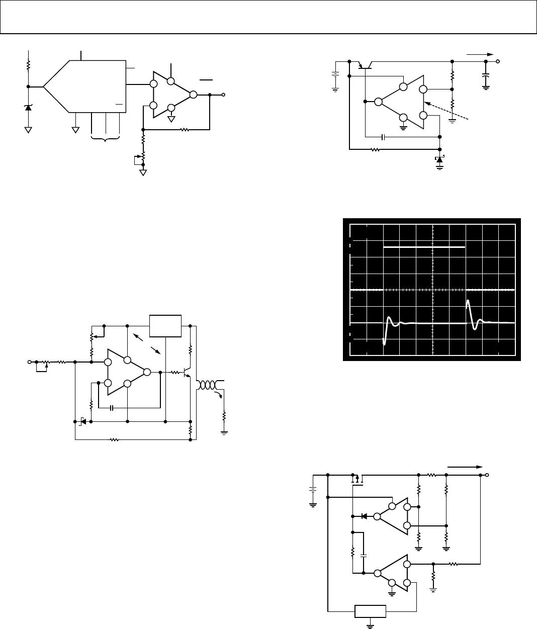
3 V LOW DROPOUT LINEAR VOLTAGE REGULATOR
Figure 29 shows a simple 3 V voltage regulator design. The
regulator can deliver 50 mA load current while allowing a
0.2 V dropout voltage. The OP295/OP495 rail-to-rail output
swing drives the MJE350 pass transistor without requiring
special drive circuitry. At no load, its output can swing less than
the pass transistor’s base-emitter voltage, turning the device
nearly off. At full load, and at low emitter-collector voltages, the
transistor beta tends to decrease. The additional base current is
easily handled by the OP295/OP495 output.
The amplifier servos the output to a constant voltage, which
feeds a portion of the signal to the error amplifier.
Higher output current, to 100 mA, is achievable at a higher
dropout voltage of 3.8 V.
V
IN
5V TO 3.2V
MJE 350
43k
AD589
1.235V
3
2
4
1
8
1000pF
I
L
< 50m
A
V
O
100µF
44.2k
1%
30.9k
1%
1/2
OP295/
OP495
+
0
0331-027
+
+
Figure 29. 3 V Low Dropout Voltage Regulator
Figure 30 shows the regulator’s recovery characteristic when its
output underwent a 20 mA to 50 mA step current change.
10
100
0%
90
1ms20mV
2V
50mA
20mA
OUTPUT
STEP
CURRENT
CONTROL
W
AVEFORM
00331-028
Figure 30. Output Step Load Current Recovery
LOW DROPOUT, 500 mA VOLTAGE REGULATOR
WITH FOLDBACK CURRENT LIMITING
Adding a second amplifier in the regulation loop, as shown in
Figure 31, provides an output current monitor as well as
foldback current limiting protection.
IRF9531
G
6V
REF43
2
4
6
2.5V
A2
A1
1
4
2
3
5
6
7
8
1N4148
I
O
(NORM) = 0.5
A
I
O
(MAX) = 1A
RSENSE
0.1
1/4W
SD
5V V
O
+
1/2
OP295/
OP495
1/2
OP295/
OP495
0.01µF
100k
5%
205k
1%
210k
1%
45.3k
1%
45.3k
1%
124k
1%
124k
1%
00331-029
+
+
Figure 31. Low Dropout, 500 mA Voltage Regulator
with Foldback Current Limiting

OP295GS-REEL

Mfr. #:
Manufacturer:
Analog Devices Inc.
Description:
Operational Amplifiers - Op Amps DUAL RAIL TO RAIL OP AMP
Lifecycle:
New from this manufacturer.
Delivery:
DHL FedEx Ups TNT EMS
Payment:
T/T Paypal Visa MoneyGram Western Union