1. General description
The BGU8L1 is, also known as the LTE1001L, a Low-Noise Amplifier (LNA) for LTE
receiver applications, available in a small plastic 6-pin extremely thin leadless package.
The BGU8L1 requires one external matching inductor.
The BGU8L1 adapts itself to the changing environment resulting from co-habitation of
different radio systems in modern cellular handsets. It has been designed for low power
consumption and optimal performance. At low jamming power levels, it delivers 14 dB
gain at a noise figure of 0.7 dB. During high-power levels, it temporarily increases its bias
current to improve sensitivity.
The BGU8L1 is optimized for 728 MHz to 960 MHz.
2. Features and benefits
Operating frequency from 728 MHz to 960 MHz
Noise figure = 0.7 dB
Gain = 14 dB
High input 1 dB compression point of 3 dBm
High in band IP3
i
of 2 dBm
Supply voltage 1.5 V to 3.1 V
Self-shielding package concept
Integrated supply decoupling capacitor
Optimized performance at a supply current of 4.6 mA
Power-down mode current consumption < 1 A
Integrated temperature stabilized bias for easy design
Require only one input matching inductor
Output DC decoupled
ESD protection on all pins (HBM > 2 kV)
Integrated matching for the output
Available in a 6-pin leadless package 1.1 mm 0.7 mm 0.37 mm; 0.4 mm pitch:
SOT1232
180 GHz transit frequency - SiGe:C technology
Moisture sensitivity level 1
BGU8L1
SiGe:C low-noise amplifier MMIC for LTE
Rev. 3 — 16 January 2017 Product data sheet
;
6
2
1
BGU8L1 All information provided in this document is subject to legal disclaimers. © NXP Semiconductors N.V. 2017. All rights reserved.
Product data sheet Rev. 3 — 16 January 2017 2 of 11
NXP Semiconductors
BGU8L1
SiGe:C low-noise amplifier MMIC for LTE
3. Applications
LNA for LTE reception in smart phones
Feature phones
Tablet PCs
RF front-end modules
4. Quick reference data
[1] E-UTRA operating band 5 (869 MHz to 894 MHz).
[2] PCB losses are subtracted.
[3] Guaranteed by device design; not tested in production.
5. Ordering information
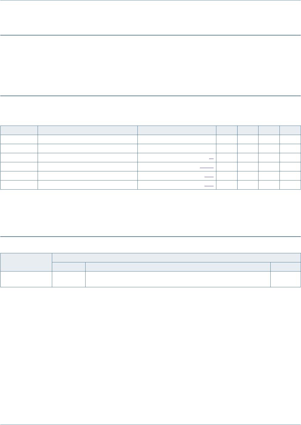
Table 1. Quick reference data
f = 882 MHz; V
CC
= 2.8 V; V
I(ENABLE)
0.8 V; T
amb
= 25 °C; input matched to 50 using a 15 nH inductor;
unless otherwise specified.
Symbol Parameter Conditions Min Typ Max Unit
V
CC
supply voltage 1.5 - 3.1 V
I
CC
supply current 2.6 4.6 6.6 mA
G
p
power gain
[1]
12.5 14.5 16.5 dB
NF noise figure
[1][2][3]
- 0.7 1.3 dB
P
i(1dB)
input power at 1 dB gain compression
[1][3]
7.0 3.0 - dBm
IP3
i
input third-order intercept point
[1][3]
3.0 +2.0 - dBm
Table 2. Ordering information
Type number Package
Name Description Version
BGU8L1 XSON6 plastic extremely thin small outline package; no leads; 6 terminals;
body 1.1 0.7 0.37 mm
SOT1232
BGU8L1 All information provided in this document is subject to legal disclaimers. © NXP Semiconductors N.V. 2017. All rights reserved.
Product data sheet Rev. 3 — 16 January 2017 3 of 11
NXP Semiconductors
BGU8L1
SiGe:C low-noise amplifier MMIC for LTE
6. Block diagram
7. Pinning information
7.1 Pinning
7.2 Pin description
Fig 1. Block diagram
DDD
%,$6&21752/
%*8[
(1$%/(


5)B,1 5)B287
9
&&
Fig 2. Pin configuration
5)B
287*1'B5)
9
&&
5)B,1
*1'
(1$%/(
7UDQVSDUHQWWRSYLHZ
DDD
Table 3. Pin description
Symbol Pin Description
GND 1 ground
V
CC
2 supply voltage
RF_OUT 3 RF output
GND_RF 4 ground RF
RF_IN 5 RF input
ENABLE 6 enable

BGU8L1X

Mfr. #:
Manufacturer:
NXP Semiconductors
Description:
RF Amplifier Low Noise Amplifier MMIC for LTE
Lifecycle:
New from this manufacturer.
Delivery:
DHL FedEx Ups TNT EMS
Payment:
T/T Paypal Visa MoneyGram Western Union

Products related to this Datasheet