BGU8L1 All information provided in this document is subject to legal disclaimers. © NXP Semiconductors N.V. 2017. All rights reserved.
Product data sheet Rev. 3 — 16 January 2017 4 of 11
NXP Semiconductors
BGU8L1
SiGe:C low-noise amplifier MMIC for LTE
8. Limiting values
[1] Stressed with pulses of 1 s in duration. V
CC
connected to a power supply of 2.8 V with 500 mA current limit.
[2] Warning: Due to internal ESD diode protection, to avoid excess current, the applied DC voltage must not exceed V
CC
+ 0.6 V or 5.0 V.
[3] The RF output is AC coupled through internal DC blocking capacitors.
9. Recommended operating conditions
10. Thermal characteristics
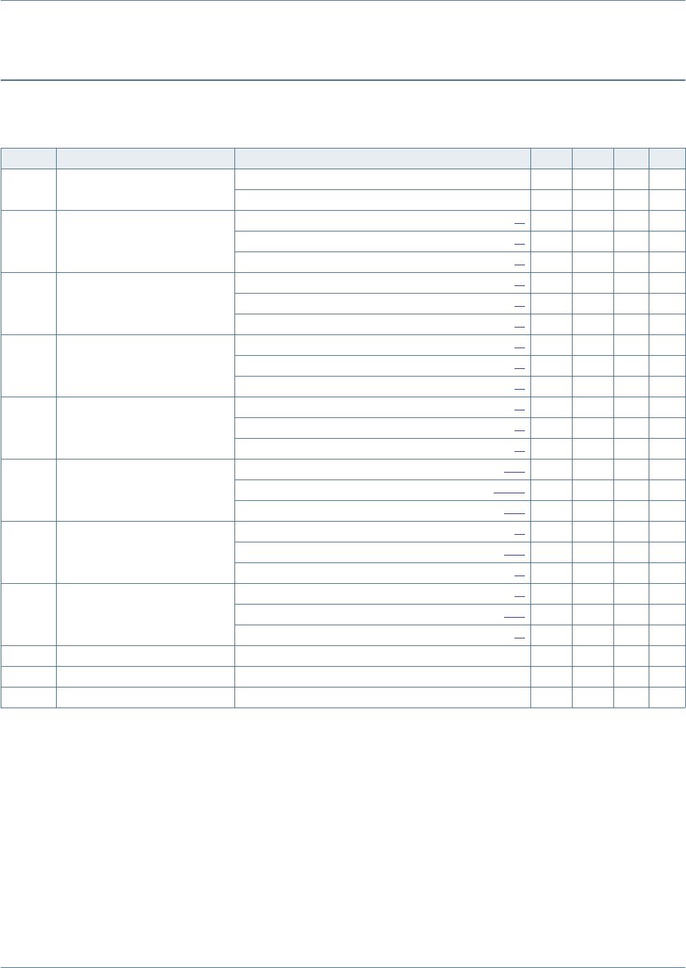
Table 4. Limiting values
In accordance with the Absolute Maximum Rating System (IEC 60134). Absolute maximum ratings are given as limiting
values of stress conditions during operation, that must not be exceeded under the worst probable conditions.
Symbol Parameter Conditions Min Max Unit
V
CC
supply voltage RF input AC coupled
[1]
0.5 +5.0 V
V
I(ENABLE)
input voltage on pin ENABLE V
I(ENABLE)
< V
CC
+ 0.6 V
[1][2]
0.5 +5.0 V
V
I(RF_IN)
input voltage on pin RF_IN DC; V
I(RF_IN)
< V
CC
+ 0.6 V
[1][2]
0.5 +5.0 V
V
I(RF_OUT)
input voltage on pin RF_OUT DC; V
I(RF_OUT)
< V
CC
+ 0.6 V
[1][2][3]
0.5 +5.0 V
P
i
input power
[1]
- 26 dBm
P
tot
total power dissipation T
sp
130 °C - 55 mW
T
stg
storage temperature 65 +150 °C
T
j
junction temperature - 150 °C
V
ESD
electrostatic discharge voltage Human Body Model (HBM)
according to ANSI/ESDA/JEDEC
standard JS-001
- 2kV
Charged Device Model (CDM)
according to JEDEC standard
JESD22-C101C
- 1kV
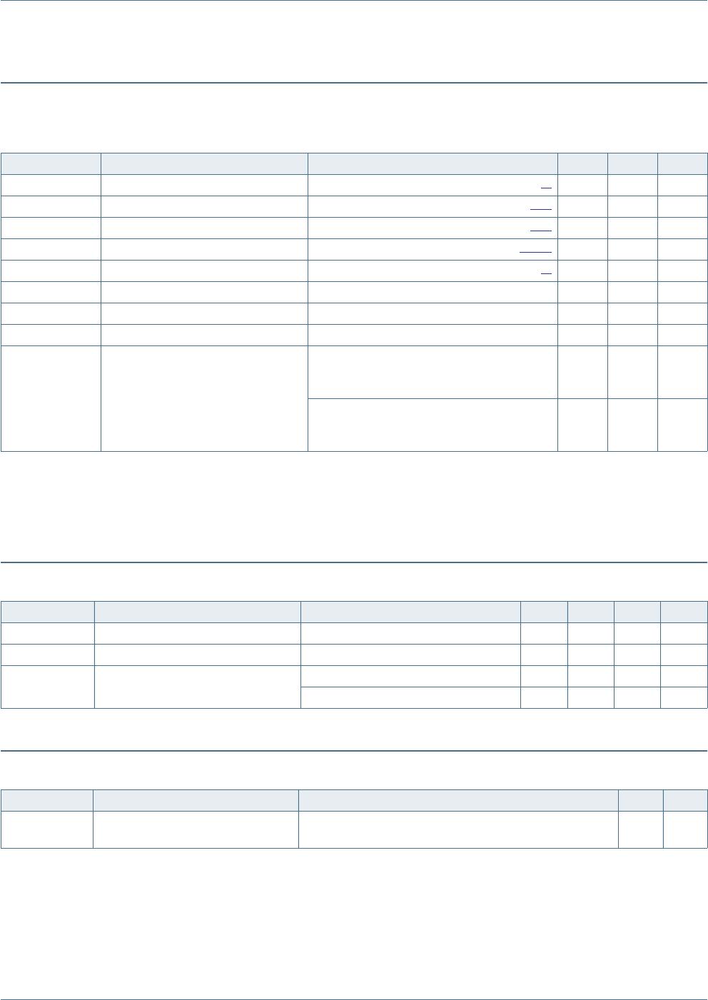
Table 5. Operating conditions
Symbol Parameter Conditions Min Typ Max Unit
V
CC
supply voltage 1.5 - 3.1 V
T
amb
ambient temperature 40 +25 +85 C
V
I(ENABLE)
input voltage on pin ENABLE OFF state - - 0.3 V
ON state 0.8 - - V
Table 6. Thermal characteristics
Symbol Parameter Conditions Typ Unit
R
th(j-sp)
thermal resistance from junction to
solder point
225 K/W