LTM8020
10
8020fd
High Temperature Considerations
The die temperature of the LTM8020 must be lower than
the maximum rating of 125°C, so care should be taken
in the layout of the circuit to ensure good heat sinking of
the LTM8020. To estimate the junction temperature, ap-
proximate the power dissipation within the LTM8020 by
applying the typical efficiency stated in this data sheet to
the desired output power, or, if you have an actual module,
by taking a power measurement. Then calculate the inter-
nal temperature rise of the LTM8020 above the surface
of the printed circuit board by multiplying the module’s
power dissipation by the thermal resistance. The actual
thermal resistance of the LTM8020 to the printed circuit
board depends upon the layout of the circuit board, but the
thermal resistance given in the Pin Configuration, which is
based upon a 25cm
2
4-layer FR4 PC board, and the Typical
Performance Characteristics can be used a guide.
Finally, be aware that at high ambient temperatures the
internal Schottky diode will have significant leakage current
increasing the quiescent current of the LTM8020.
BIAS Pin Considerations
The BIAS pin is used to provide drive power for the internal
power switching stage and operate internal circuitry. For
proper operation, it must be powered by at least 3V. If the
output voltage is programmed to be 3V or higher, simply
tie BIAS to V
OUT
. If V
OUT
is less than 3V, BIAS can be tied
to V
IN
or some other voltage source. In all cases, ensure
that the maximum voltage at the BIAS pin is both less than
25V and the sum of V
IN
and BIAS is less than 47V. If BIAS
power is applied from a remote or noisy voltage source, it
may be necessary to apply a decoupling capacitor locally
to the LTM8020.
APPLICATIONS INFORMATION
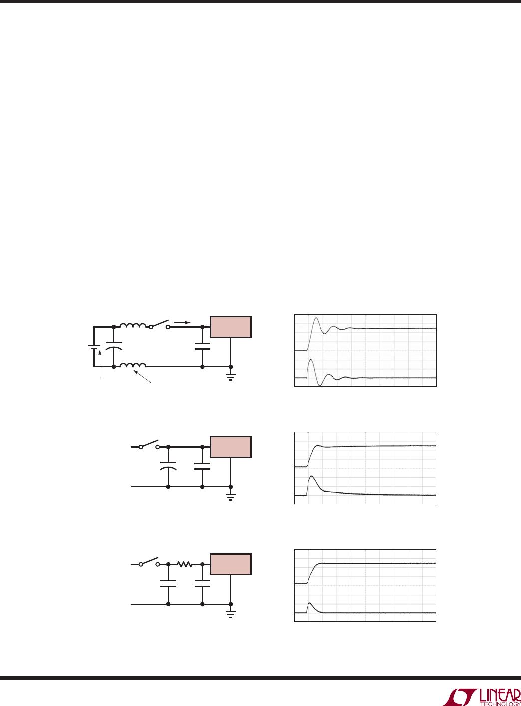
Figure 4. A Well Chosen Input Network Prevents Input Voltage Overshoot and Ensures
Reliable Operation When the LTM8020 is Connected to a Live Supply
+
LTM8020
2.2μF
V
IN
10V/DIV
I
IN
10A/DIV
V
IN
10V/DIV
I
IN
10A/DIV
V
IN
10V/DIV
I
IN
10A/DIV
10μs/DIV
10μs/DIV
10μs/DIV
V
IN
CLOSING SWITCH
SIMULATES HOT PLUG
I
IN
(4a)
(4b)
(4c)
LOW
IMPEDANCE
ENERGIZED
24V SUPPLY
STRAY
INDUCTANCE
DUE TO 6 FEET
(2 METERS) OF
TWISTED PAIR
+
LTM8020
2.2μF
10μF
35V
AI.EI.
LTM8020
2.2μF0.1μF
8020 F04
LTM8020
11
8020fd
APPLICATIONS INFORMATION
Table 1. Recommended External Component Values and Configuration
V
IN
RANGE V
OUT
C
IN
C
OUT
R
ADJ
BIAS CONNECTION
4.5V - 36V 1.25V 2.2μF 50V 1206 X7R 47μF 6.3V 1206 X5R Open >2V, < 25V
4.5V - 36V 1.5V 2.2μF 50V 1206 X7R 47μF 6.3V 1206 X5R 2.43M >2V, < 25V
4.5V - 36V 1.8V 2.2μF 50V 1206 X7R 47μF 6.3V 1206 X5R 1.1M >2V, < 25V
4.5V - 36V 2.5V 2.2μF 50V 1206 X7R 22μF 6.3V 1206 X7R 499k V
OUT
4.5V - 36V 3.3V 2.2μF 50V 1206 X7R 10μF 6.3V 1206 X7R 301k V
OUT
6.5V - 36V 5V 2.2μF 50V 1206 X7R 10μF 6.3V 1206 X7R 165k V
OUT
4.5V - 15V 1.25V 2.2μF 16V 0805 X7R 22μF 6.3V 1206 X7R Open V
IN
4.5V - 15V 1.5V 2.2μF 16V 0805 X7R 10μF 6.3V 0805 X7R 2.43M V
IN
4.5V - 15V 1.8V 2.2μF 16V 0805 X7R 10μF 6.3V 0805 X7R 1.1M V
IN
4.5V - 15V 2.5V 2.2μF 16V 0805 X7R 10μF 6.3V 0805 X7R 499k V
IN
4.5V - 15V 3.3V 2.2μF 16V 0805 X7R 10μF 6.3V 0805 X7R 301k V
OUT
6.5V - 15V 5V 2.2μF 16V 0805 X7R None 165k V
OUT
9V - 24V 1.25V 1μF 25V 0805 X7R 47μF 6.3V 0805 X5R Open V
IN
9V - 24V 1.5V 1μF 25V 0805 X7R 47μF 6.3V 0805 X7R 2.43M V
IN
9V - 24V 1.8V 1μF 25V 0805 X7R 10μF 6.3V 0805 X7R 1.1M V
IN
9V - 24V 2.5V 1μF 25V 0805 X7R 10μF 6.3V 0805 X7R 499k V
IN
9V - 24V 3.3V 1μF 25V 0805 X7R 10μF 6.3V 0805 X7R 301k V
OUT
9V - 24V 5V 4.7μF 25V 0805 X7R 10μF 6.3V 0805 X5R 165k V
OUT
18V - 36V 1.25V 2.2μF 50V 1206 X7R 47μF 6.3V 1206 X5R Open >2V, <25V
18V - 36V 1.5V 2.2μF 50V 1206 X7R 47μF 6.3V 1206 X5R 2.43M >2V, <25V
18V - 36V 1.8V 2.2μF 50V 1206 X7R 22μF 6.3V 1206 X7R 1.1M >2V, <25V
18V - 36V 2.5V 2.2μF 50V 1206 X7R 10μF 6.3V 0805 X7R 499k V
OUT
18V - 36V 3.3V 2.2μF 50V 1206 X7R 10μF 6.3V 0805 X7R 301k V
OUT
18V - 36V 5V 2.2μF 50V 1206 X7R 10μF 6.3V 0805 X7R 165k V
OUT
3.3V - 30V –3.3V 2.2μF 50V 1206 X7R 22μF 6.3V 0805 X7R 301k V
OUT
5V - 30V –5V 2.2μF 50V 1206 X7R 10μF 6.3V 0805 X7R 165k V
OUT
Minimum Input Voltage
The LTM8020 is a step-down converter, so a minimum
amount of headroom is required to keep the output in
regulation. For most applications at full load, the input
needs to be at least 1.5V above the desired output. In
addition, the input voltage required to turn on depends
upon how the SHDN pin is tied. It takes more input voltage
to turn on if SHDN is tied to V
IN
than if the turn-on is
controlled by raising SHDN when V
IN
is in the required
operating range. A graph of the input voltage required to
turn the LTM8020 on when SHDN is tied to V
IN
or when
SHDN is switched is given in the Typical Performance
Characteristics section.
Electromagnetic Compliance
The LTM8020 was evaluated by an independent nationally
recognized test lab and found to be compliant with EN55022
class B: 2006 by a wide margin. A sample graph of the
LTM8020’s radiated EMC performance is given in the
Typical Performance Characteristics section, while further
data, operating conditions and test setup are detailed in
the electromagnetic compatibility test report, available
on the Linear Technology website. Conducted emissions
requirements may be met by adding an appropriate input
power line filter. The proper implementation of this filter
depends upon the system operating and performance
conditions as a whole, of which the LTM8020 is typically
only a component, so conducted emissions are not
addressed at this level.
LTM8020
12
8020fd
V
IN
(V)
0
0
I
LOAD
(mA)
50
100
150
200
10 155203025
8020 TA08
250
V
IN
V
OUT
LTM8020
BIAS
SHDN
10μF
X5R
165k
1%
2.2μF
–5V
V
IN
*
5V TO 30V
8020 TA06
ADJ
GND
–5V
85μA
OPTIONAL
SCHOTTKY
CLAMP
–5V Positive-to-Negative Converter
V
IN
V
OUT
LTM8020
BIASSHDN
165k
1%
2.2μF
V
IN
*
6.5V TO 15V
8020 TA05
GND ADJ
V
OUT
5V
200mA
5V Step-Down Converter (No Output Capacitor Required)
TYPICAL APPLICATIONS
V
IN
V
OUT
LTM8020
SHDN
47μF
X5R
F
V
IN
*
4.5V TO 24V
8020 TA02
GND ADJ
V
OUT
1.25V
200mA
BIAS
V
IN
V
OUT
LTM8020
BIASSHDN
10μF
X5R
301k
1%
F
V
IN
*
4.5V TO 36V
8020 TA04
GND ADJ
V
OUT
3.3V
200mA
1.25V Step-Down Converter 3.3V Step-Down Converter
V
IN
V
OUT
LTM8020
SHDN
BIAS
22μF
X7R
1.1M
1%
2.2μF
V
IN
*
4.5V TO 15V
8020 TA03
GND ADJ
V
OUT
1.8V
200mA
1.8V Step-Down Converter
–5V Positive-to-Negative Converter
Output vs Input Voltage
*
* RUNNING VOLTAGE RANGE. PLEASE REFER TO APPLICATIONS INFORMATION FOR START-UP DETAILS

LTM8020IV#PBF

Mfr. #:
Manufacturer:
Analog Devices / Linear Technology
Description:
Switching Voltage Regulators 36V, 200mA Step-down Module Regulator
Lifecycle:
New from this manufacturer.
Delivery:
DHL FedEx Ups TNT EMS
Payment:
T/T Paypal Visa MoneyGram Western Union

Products related to this Datasheet