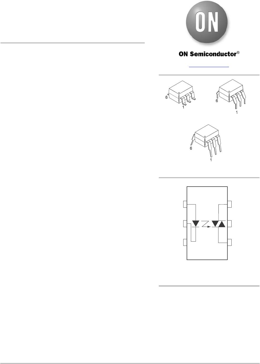
MOC3010M, MOC3011M, MOC3012M, MOC3020M, MOC3021M, MOC3022M, MOC3023M
www.onsemi.com
2
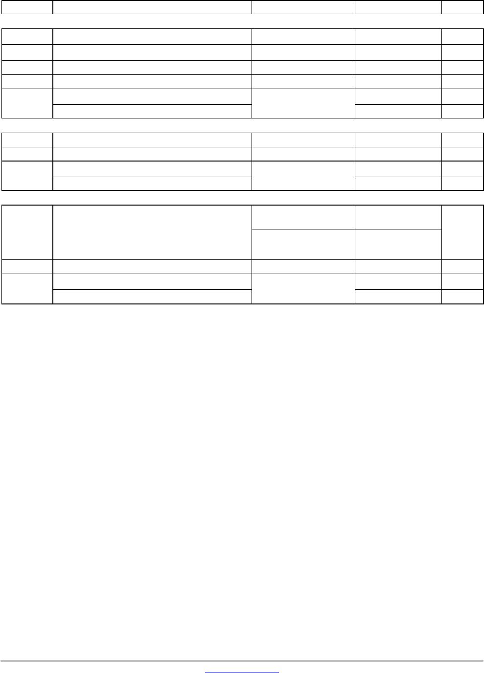
SAFETY AND INSULATION RATINGS
As per DIN EN/IEC 60747−5−5, this optocoupler is suitable for “safe electrical insulation” only within the safety limit data. Compliance with
the safety ratings shall be ensured by means of protective circuits.
Parameter
Characteristics
Installation Classifications per DIN VDE 0110/1.89 Table 1, For
Rated Mains Voltage
< 150 V
RMS
I–IV
< 300 V
RMS
I–IV
Climatic Classification 40/85/21
Pollution Degree (DIN VDE 0110/1.89) 2
Comparative Tracking Index 175
Symbol Parameter Value Unit
V
PR
Input−to−Output Test Voltage, Method A, V
IORM
x 1.6 = V
PR
, Type and Sample Test
with t
m
= 10 s, Partial Discharge < 5 pC
1275
Vpeak
Input−to−Output Test Voltage, Method B, V
IORM
x 1.875 = V
PR
, 100% Production Test
with t
m
= 1 s, Partial Discharge < 5 pC
1594
Vpeak
V
IORM
Maximum Working Insulation Voltage 850
Vpeak
V
IOTM
Highest Allowable Over−Voltage 6000
Vpeak
External Creepage
≥ 7
mm
External Clearance
≥ 7
mm
External Clearance (for Option TV, 0.4” Lead Spacing)
≥ 10
mm
DTI Distance Through Insulation (Insulation Thickness)
≥ 0.5
mm
R
IO
Insulation Resistance at T
S
, V
IO
= 500 V
> 10
9
W