1
DEMO MANUAL DC094
DESIGN READY SWITCHER
LTC1435 Constant Frequency
Synchronous DC/DC Converter
DESCRIPTIO
U
, LTC and LT are registered trademarks of Linear Technology Corporation.
This results in a power supply that has very high
efficiency, low ripple and fast transient response. At
low output currents the LTC1435 automatically switches
to Burst Mode
TM
operation to reduce switching losses
and maintain high operating efficiencies. Additionally,
the supply current can be shut down to less than
20µA with an input voltage of 10V. This feature is an
absolute necessity to maximize battery life in portable
applications. Gerber files for this circuit board are avail-
able. Call the LTC factory.
Burst Mode is a trademark of Linear Technology Corporation.
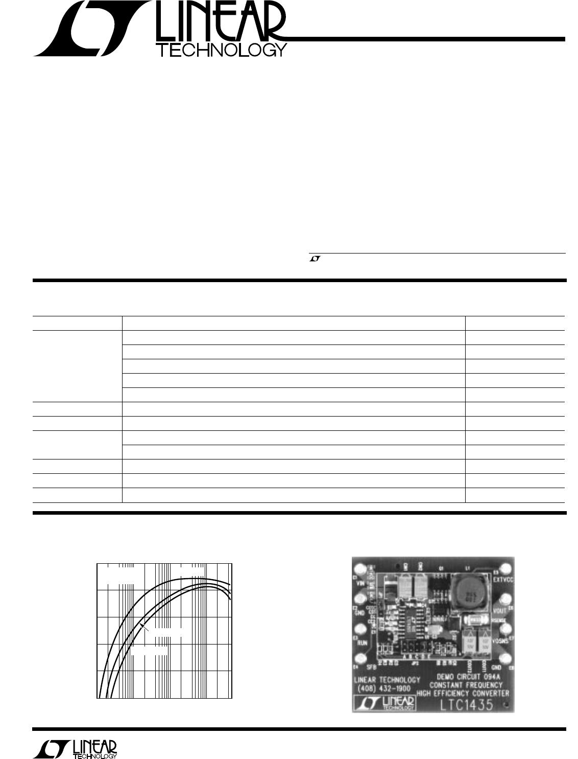
TYPICAL PERFOR A CE CHARACTERISTICS A D BOARD PHOTO
U
U
W
Efficiency
LOAD CURRENT (mA)
1
EFFICIENCY (%)
100
90
80
70
60
50
10 100
DM094 TPC01
1000 4000
V
IN
= 10V
SFB = INT V
CC
V
OUT
= 5V
V
OUT
= 2.5V
V
OUT
= 3.3V
PERFOR A CE SU ARY
UWWW
Operating Temperature Range 0
°
C to 50
°
C
Input Voltage Range
Maximum Input Voltage (Limited by External MOSFET and Input Capacitor) 4.5V to 28V
Output Output Voltage (Jumper Selectable) 1.8V, 2.5V, 2.9V, 3.3V, 5V
Maximum Output Current (Continuous) 3A
Maximum Output Current (Peak) 3.5A
Typical Output Ripple at 10MHz Bandwidth (Burst Mode
Operation) I
O
= 100mA 50mV
P-P
Typical Output Ripple at 10MHz Bandwidth (Continuous) I
O
= 1A 35mV
P-P
V
IN
Line Regulation, 6V to 20V 0.002%/V
I
OUT
Load Regulation, No Load to Full Rated Output 1%
I
Q
Supply Current with No Load at 10V Input (Typical), SFB = INT V
CC
, EXT V
CC
= 5V 50µA
Supply Current in Shutdown (Typical), V
IN
= 10V 15µA
I
EXTVCC
EXT V
CC
Pin Current, V
EXTVCC
= 5V, V
IN
= 10V, No Load 650µA
V
RUN
Run Pin Threshold (Typical) 1.3V
Frequency Operating Frequency (Typical), C
OSC
= 68pF
170kHz
DM094 BP
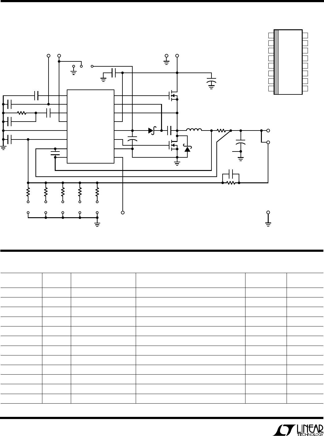
Demonstration Circuit 094 is a constant frequency step-
down (buck) regulator implemented entirely in surface
mount using the LTC
®
1435 switching regulator controller.
The output voltage is programmable from 1.8V to 5V via
a jumper. The input voltage can range from 4.5V to 28V
(limited by the external MOSFETs). The circuit highlights
the capabilities of the LTC1435 which uses a current
mode, constant frequency architecture to switch a pair of
N-channel power MOSFETs while providing 99% maxi-
mum duty cycle. Operating efficiencies exceeding 90%
are obtained.
2
DEMO MANUAL DC094
DESIGN READY SWITCHER
PACKAGE A D SCHE ATIC DIAGRA SM
W UW
TOP VIEW
S PACKAGE
16-LEAD PLASTIC SO
1
2
3
4
5
6
7
8
16
15
14
13
12
11
10
9
C
OSC
RUN/SS
I
TH
SFB
SGND
V
OSENSE
SENSE
SENSE
+
TG
BOOST
SW
V
IN
INT V
CC
BG
PGND
EXT V
CC
1
2
3
4
5
6
7
8
16
15
14
13
12
11
10
9
+
+
C
OSC
RUN/SS
I
TH
SFB
SGND
V
OSENSE
SENSE
SENSE
+
TG
BOOST
SW
V
IN
INT V
CC
BG
PGND
EXT V
CC
C
OSC
68pF
E3
RUN
E4
SFB
E5
EXT V
CC
C
OUT
100µF
10V
× 2
+
C
IN
22µF
35V
× 2
C
C
330pF
Q2
Si4412DY
Q1
Si4412DY
D2
MBRS140T3
SGND
DM 094 F01
L1
10µH
R1
35.7k
1%
R
SENSE
0.033
V
IN
4.5V TO 28V
C3
4.7µF
16V
R2
69.8k
1%
C4
0.1µF
C6
100pF
C2
0.1µF
JP1
INT V
CC
GND
D1
CMDSH-3
U1
LTC1435
C5
1000pF
R
C
, 10k
C
C2
, 51pF
C1, 100pF
C
SS
, 0.1µF
E1
E6
V
OUT
E7
V
OSENSE
E8
GND
E2
JP2A
1.8V
R3
32.4k
1%
JP2B
2.5V
R4
24.9k
1%
JP2C
2.9V
R5
20k
1%
JP2D
3.3V
R6
11k
1%
JP2E
5V
Figure 1. LTC1435 Constant Frequency, High Efficiency Converter
PARTS LIST
REFERENCE
DESIGNATOR QUANTITY PART NUMBER DESCRIPTION VENDOR TELEPHONE
C
C
1 08055A331KAT1A 330pF 50V 10% NPO Chip Capacitor AVX (803) 448-9411
C
C2
1 08055A510KAT1A 51pF 50V 10% NPO Chip Capacitor AVX (803) 448-9411
C
IN1
, C
IN2
2 TPSE226M035 22µF 35V 20% Tantalum Capacitor AVX (803) 448-9411
C
OSC
1 08055A680JAT1A 68pF 50V 5% NPO Chip Capacitor AVX (803) 448-9411
C
OUT1
, C
OUT2
2 TPSD107M010R0080 100µF 10V 20% Tantalum Capacitor AVX (803) 448-9411
C1, C6 2 08055A101KAT1A 100pF 50V 10% NPO Chip Capacitor AVX (803) 448-9411
C2, C4, C
SS
3 08055G104KAT1A 0.1µF 50V 10% Y5V Chip Capacitor AVX (803) 448-9411
C3 1 TAJB475M016 4.7µF 16V 20% Tantalum Capacitor AVX (803) 448-9411
C5 1 08055C102KAT1A 1000pF 50V 10% X7R Chip Capacitor AVX (803) 448-9411
D1 1 CMDSH-3 BVR = 30V Schottky Diode Central (516) 435-1110
D2 1 MBRS140T3 BVR = 40V Schottky Diode Motorola (602) 244-3576
E1 to E8 8 1502-2 Turret Terminal Keystone (718) 956-8900
LTC1435CS
3
DEMO MANUAL DC094
DESIGN READY SWITCHER
PARTS LIST
REFERENCE
DESIGNATOR QUANTITY PART NUMBER DESCRIPTION VENDOR TELEPHONE
JP1 1 2802S-03-G2 2mm Pin Header Comm Con (818) 301-4200
JP2 1 2802S-10-G2 2mm Pin Header Comm Con (818) 301-4200
L1 1 CDRH125-10 10µH Inductor Sumida (708) 956-0666
CDRH127-10 10µH Inductor (Alternate) Sumida
Q1, Q2 2 Si4412DY N-Channel MOSFET Siliconix (800) 554-5565
R1 1 CR21-3572F-T 35.7k 1/10W 1% Chip Resistor AVX (803) 448-9411
R2 1 CR21-6982F-T 69.8k 1/10W 1% Chip Resistor AVX (803) 448-9411
R3 1 CR21-3242F-T 32.4k 1/10W 1% Chip Resistor AVX (803) 448-9411
R4 1 CR21-2492F-T 24.9k 1/10W 1% Chip Resistor AVX (803) 448-9411
R5 1 CR21-2002F-T 20k 1/10W 1% Chip Resistor AVX (803) 448-9411
R6 1 CR21-1102F-T 11k 1/10W 1% Chip Resistor AVX (803) 448-9411
R
C
1 CR21-103J-T 10k 1/10W 5% Chip Resistor AVX (803) 448-9411
R
SENSE
1 LR2010-01-R033-F 0.033 1/2W 1% Resistor IRC (512) 992-7900
U1 1 LTC1435CS 16-Lead Narrow Small Outline IC LTC (408) 432-1900
2 CCIJ2mm-138-G Jumper Comm Con (818) 301-4200
QUICK START GUIDE
This demonstration board is easy to set up to evaluate the
performance of the LTC1435. Please follow the procedure
outlined below for proper operation.
1. Refer to Figure 3 for proper arrangement of monitoring
equipment for correct measurement equipment setup.
2. Connect the input power supply to the V
IN
and GND
terminals on the left-hand side of the board. Do not
increase V
IN
over 28V or the MOSFET(s)
will be dam-
aged
. At lower output voltages (V
OUT
< 2.5V) the maxi-
mum input voltage must be decreased. See Table 1.
3. Connect the load between the V
OUT
and GND terminals
on the right side of the board.
4. The RUN pin can be left unconnected. To shut down the
LTC1435 tie this pin to ground.
5. When the 5V output voltage option is selected externally
connect EXT V
CC
to V
OUT
.
6. Set the jumper JP1 so that SFB is connected to
INT V
CC
.
7. Set the desired output voltage with jumper JP2 shown
in Figure 2 and Table 1.
Table 1. Maximum Allowable Input Voltage vs Selected
Output Voltage
MAXIMUM INPUT
POSITION OUTPUT VOLTAGE VOLTAGE
A 1.8V 18V
B 2.5V 24V
C 2.9V 28V
D 3.3V 28V
E 5V 28V
Figure 2. Output Voltage Selection (JP2)
(3.3V Position Shown)
JP2
ABCDE
2.5V
1.8V
2.9V
3.3V 5V
DM094 F02

DC094A

Mfr. #:
Manufacturer:
Analog Devices Inc.
Description:
Power Management IC Development Tools LTC1435 - CONSTANT FREQ HIGH EFF. 3A CON
Lifecycle:
New from this manufacturer.
Delivery:
DHL FedEx Ups TNT EMS
Payment:
T/T Paypal Visa MoneyGram Western Union

Products related to this Datasheet