4
DEMO MANUAL DC094
DESIGN READY SWITCHER
I TRODUCTIO
U U
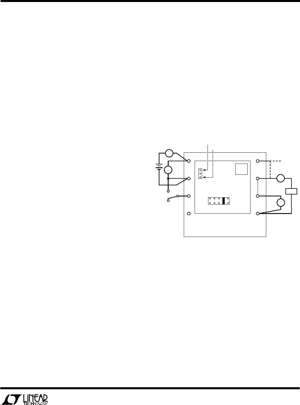
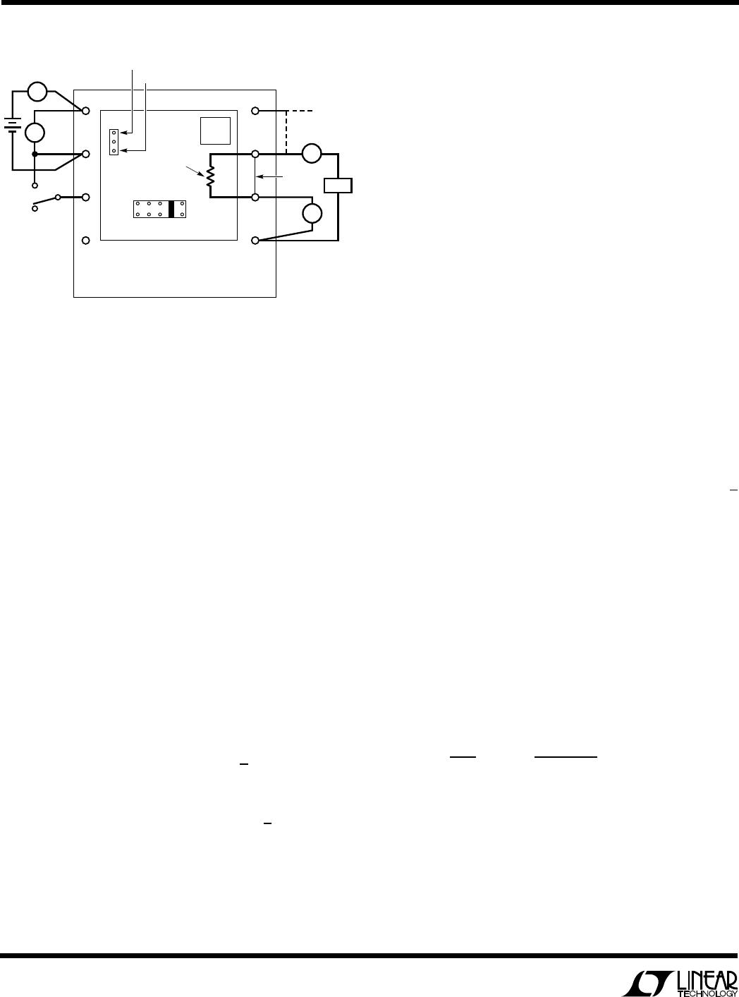
The circuit in Figure 1 highlights the capabilities of the
LTC1435. The application circuit is set up for a variety of
output voltages. Output voltages from 1.8V to 5V are
available by selecting the appropriate jumper position.
The LTC1435 is a synchronous step-down switching
regulator controller which drives external N-channel power
MOSFETs using a fixed frequency architecture. Burst
Mode operation provides high efficiency at low load cur-
rents. Operating efficiencies typically exceed 90% over
three decades of load current range. A maximum high duty
cycle limit of 99% provides low dropout operation which
extends operating time in battery-operated systems.
The use of small spring-clip leads are very convenient for
small-signal bench testing and voltage measurements,
but should not be used with the high currents associated
with this circuit. Soldered wire connections are required to
properly ascertain the performance of the PC board.
This demonstration unit is intended for the evaluation of
the LTC1435 switching regulator IC and was not designed
for any other purpose.
OPERATIO
U
The operating frequency is set by an external capacitor
C
OSC
, allowing maximum flexibility in optimizing effi-
ciency. In this application the frequency is set to 170kHz.
A secondary winding feedback control pin SFB inhibits
Burst Mode which reduces noise and RF interference.
Soft start is provided by an external capacitor C
SS
which
can be used to properly sequence supplies. The operating
current level is user-programmable via an external current
sense resistor and is set to 3A. Short-circuit current limit
is set approximately to 4A.
This demo board is optimized for 3.3V outputs. A wide
input supply range allows operation from 4.5V to 28V for
V
OUT
voltages of 3.3V and 5V. Because this board allows
for a wide output voltage range (1.8V to 5V) and the
operating frequency remains constant at 170kHz, there is
a duty cycle induced limit on the maximum input voltage
when low output voltages are selected (V
OUT
< 2.9V). This
is necessary for an adequate turn-on time for the top
MOSFET with the required duty cycle at a given frequency.
If a higher input supply voltage is required together with
low output voltage, the operating frequency can be de-
creased by increasing C
OSC
.
Main Control Loop
The LTC1435 uses a constant frequency, current mode
step-down architecture. Current mode operation was
judged to be mandatory for its well-known advantages of
clean start-up, accurate current limit and excellent line and
load regulation.
During normal operation, the top MOSFET is turned on
each cycle when the oscillator sets a latch and turned off
when the main current comparator resets the latch. The
peak inductor current is controlled by the voltage on the
I
TH
pin, which is the output of error amplifier EA.
The V
OSENSE
pin allows EA to receive an output feedback
voltage V
FB
from an external resistive divider. When the
load current increases, it causes a slight decrease in V
FB
relative to the 1.19V reference, which in turn causes the I
TH
voltage to increase until the average inductor current
matches the new load current. While the top MOSFET is
off, the bottom MOSFET is turned on until either the
inductor current starts to reverse or the beginning of the
next cycle.
The top MOSFET driver is biased from floating bootstrap
capacitor C4, which normally is recharged during each off
cycle. However, when V
IN
decreases to a voltage close to
V
OUT
, the loop may enter dropout and attempt to turn on
the top MOSFET continuously. The dropout detector counts
the number of oscillator cycles that the top MOSFET
remains on and periodically forces a brief off period to
allow C4 to recharge.
A built-in comparator guards against transient overshoots
> 7.5% by turning off the top MOSFET and keeping it off
until the fault is removed.
5
DEMO MANUAL DC094
DESIGN READY SWITCHER
OPERATIO
U
Low Current Operation
The LTC1435 is capable of Burst Mode operation in which
the external MOSFETs operate intermittently based on
load demand. If the voltage across R
SENSE
does not exceed
approximately 20mV for one full cycle, then on following
cycles the top and bottom drives are disabled. This contin-
ues until the I
TH
voltage exceeds 0.6V, which causes drive
to be returned to the top MOSFET on the next cycle.
Two conditions can force continuous synchronous opera-
tion, even when the load current would otherwise dictate
low current operation. One is when the common mode
voltage of the Sense
+
and Sense
pins is below 1.4V, and
the other is when the SFB pin is below 1.19V. See the SFB
pin function description.
INT V
CC
/EXT V
CC
Power
Power for the top and bottom MOSFET drivers and most
of the other LTC1435 circuitry is derived from INT V
CC
pin.
When the EXT V
CC
pin is left open, an internal 5V low
dropout regulator supplies INT V
CC
power. If EXT V
CC
is
taken above 4.7V, the 5V regulator is turned off and an
internal switch is turned on to connect EXT V
CC
to INT V
CC
.
This allows the INT V
CC
power to be derived from a high
efficiency external source such as the output of the regu-
lator itself or a secondary winding, as described in the
LTC1435 data sheet.
When the 5V output voltage option is selected (JP2E
installed) the EXT V
CC
pin should be externally connected
to V
OUT
.
HOW TO MEASURE VOLTAGE REGULATION
When trying to measure voltage regulation, remember
that all measurements must be taken at the point of
regulation. This point is where the LTC1435’s control loop
looks for the information to keep the output voltage
constant. In this demonstration board this information
point occurs between Pin 5 of the LTC1435, the signal
ground, and the output side of R1. These points corre-
spond to the V
OSENSE
(E7) terminal of the board. Output
voltage test leads should be attached directly to this
terminal. The load should be placed across V
OUT
(E6) to
GND (E8). Measurements
should not
be taken at the end
of test leads at the load. Refer to Figure 3 for the proper
monitoring equipment configuration.
This applies to line regulation (input to output voltage
regulation) as well as load regulation tests. In doing line
regulation tests always look at the input voltage across the
input terminals.
For the purposes of these tests the demonstration circuit
should be fed from a regulated DC bench supply so
additional variation on the DC input does not add an error
to the regulation measurements.
Figure 3. Proper Measurement Setup
REMOTE OUTPUT VOLTAGE SENSING
Remote output voltage sensing can be accomplished by
modifying the PC board. A small PC trace connecting V
OUT
to V
OSENSE
must be cut as shown in Figure 4. An external
connection from V
OSENSE
directly across the load must be
made. To prevent uncertainty, solder a 10 resistor
across the V
OUT
and V
OSENSE
terminals. Never, under any
circumstance, allow V
OSENSE
to float!
JP1
V
IN
V
IN
GND
RUN
OPEN
OFF
RUN
SFB
LINEAR TECHNOLOGY
(408) 432-1900
DEMO CIRCUIT 094A
CONSTANT FREQUENCY
HIGH EFFICIENCY CONVERTER
LTC1435
EXT V
CC
V
OUT
I
OUT
V
OUT
V
OSENSE
GND
BURST MODE ENABLED
BURST MODE DISABLED
EXTERNAL
SOURCE
JP2
ABCDE
DM094 F03
+
+
A
I
IN
+
A
+
V
+
V
V 10V
LOAD
6
DEMO MANUAL DC094
DESIGN READY SWITCHER
OPERATIO
U
However, for 3.3V and other lower voltage regulators,
additional circuitry is required to derive INT V
CC
power
from the output.
The following list summarizes the four possible connec-
tions for EXT V
CC:
1. EXT V
CC
Left Open (or Grounded). This will cause
INT V
CC
to be powered from the internal 5V regulator
resulting in an efficiency penalty of up to 10% at high
input voltages.
2. EXT V
CC
Connected Directly to V
OUT
. This is the normal
connection for a 5V regulator and provides the highest
efficiency.
3. EXT V
CC
Connected to an Output-Derived Boost Net-
work. For 3.3V and other low voltage regulators, effi-
ciency gains can still be realized by connecting EXT V
CC
to an output-derived voltage which has been boosted to
greater than 4.7V. See the LTC1435 data sheet for
further details.
4. EXT V
CC
Connected to an External Supply. If an external
supply is available in the 5V to 10V range (EXT V
CC
<
V
IN
), it may be used to power EXT V
CC
providing an
efficiency boost.
SFB Pin Function (Burst Mode Disable)
When the SFB (E4) pin drops below its ground-referenced
1.19V threshold, continuous mode operation is forced
(Burst Mode is inhibited). In continuous mode the
N-channel main and synchronous switches are continu-
ously switched irrelevant of the load on the main output.
This reduces noise and interference but impacts effi-
ciency. Jumper JP1 sets the voltage on SFB and is set as
follows:
SFB Condition
GND Burst Mode Inhibited
INT V
CC
Burst Mode Enabled
In addition to providing a logic input to force continuous
synchronous operation, the SFB pin provides a means to
regulate a flyback winding output. See the LTC1435 data
sheet for additional information.
INT V
CC
Regulator
An internal P-channel low dropout regulator produces the
5V supply which powers the drivers and internal circuitry
within the LTC1435. The INT V
CC
pin can supply up to
15mA (this includes the gate drive currents). External
loading of the INT V
CC
pin may be up to 10mA. At high
input voltages the maximum junction temperature rating
for the LTC1435 may be exceeded if too large an external
load is placed on INT V
CC
. See the LTC1435 data sheet for
further details.
EXT V
CC
Connection
The LTC1435 contains an internal P-channel MOSFET
switch connected between the EXT V
CC
and INT V
CC
pins.
The switch closes and supplies the INT V
CC
power when-
ever the EXT V
CC
pin is above 4.7V and remains closed
until EXT V
CC
drops below 4.5V. This allows the MOSFET
driver and control power to be derived from the output
during normal operation (4.7V < V
OUT
< 9V) and from the
internal regulator when the output is out of regulation
(start-up, short circuit). Do not apply greater than 10V to
the EXT V
CC
pin and ensure that EXT V
CC
< V
IN
.
Significant efficiency gains can be realized by powering
INT V
CC
from the output, since the V
IN
current resulting
from the driver and control currents will be scaled by a
factor of (Duty Cycle)/(Efficiency). For 5V regulators this
simply means connecting the EXT V
CC
pin directly to V
OUT
.
JP1
V
IN
V
IN
GND
RUN
OPEN
OFF
RUN
SFB
LINEAR TECHNOLOGY
(408) 432-1900
DEMO CIRCUIT 094A
CONSTANT FREQUENCY
HIGH EFFICIENCY CONVERTER
LTC1435
EXT V
CC
V
OUT
I
OUT
V
OUT
CUT THIS
TRACE
ADD THIS
RESISTOR
10
V
OSENSE
GND
BURST MODE ENABLED
BURST MODE DISABLED
EXTERNAL
SOURCE
JP2
ABCDE
DM094 F04
+
+
A
I
IN
+
A
+
V
+
V
V 10V
LOAD
Figure 4. Remote Output Voltage Sense

DC094A

Mfr. #:
Manufacturer:
Analog Devices Inc.
Description:
Power Management IC Development Tools LTC1435 - CONSTANT FREQ HIGH EFF. 3A CON
Lifecycle:
New from this manufacturer.
Delivery:
DHL FedEx Ups TNT EMS
Payment:
T/T Paypal Visa MoneyGram Western Union

Products related to this Datasheet