Micrel, Inc. MIC2940A/2941A
July 2007
4
M9999-071307
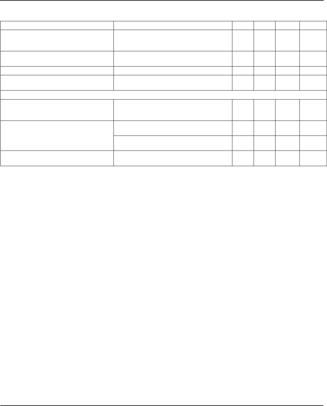
Electrical Characteristics (MIC2941A Only)
Parameter Condition Min Typ Max Units
Reference Voltage
(Note 8)
1.223
1.210
1.204
1.235
1.247
1.260
1.266
V
V
V
Adjust Pin Bias Current
20
40
60
nA
nA
Reference Voltage Temperature Coefficient 20 ppm/°C
Adjust Pin Bias Current Temperature
Coefficient
0.1 nA/°C
Shutdown Input
Input Logic Voltage
Low (ON)
High (OFF)
2.0
1.3
0.7
V
V
V
V
SHUTDOWN
= 2.4V 30
50
100
µA
µA
Shutdown Pin Input Current
V
SHUTDOWN
= 26V 450
600
750
µA
µA
Regulator Output Current in Shutdown
(Note 10)
3
30
60
µA
µA
Notes:
1. Absolute maximum ratings indicate limits beyond which damage to the component may occur. Electrical specications do not apply when operating
the device outside of its rated operating conditions. The maximum allowable power dissipation is a function of the maximum junction temperature,
T
J(MAX)
, the junction-to-ambient thermal resistance, θ
JA
, and the ambient temperature, T
A
. The maximum allowable power dissipation at any ambient
temperature is calculated using: P
(MAX)
= (T
J(MAX)
– T
A
) / θ
JA
. Exceeding the maximum allowable power dissipation will result in excessive die
temperature, and the regulator will go into thermal shutdown.
2. Output voltage temperature coefcient is dened as the worst case voltage change divided by the total temperature range.
3. Regulation is measured at constant junction temperature using low duty cycle pulse testing. Changes in output voltage due to heating effects are
covered by the thermal regulation specication.
4. Dropout Voltage is dened as the input to output differential at which the output voltage drops 100 mV below its nominal value measured at 1V
differential. At low values of programmed output voltage, the minimum input supply voltage of 4.3V over temperature must be taken into account.
5. Ground pin current is the regulator quiescent current. The total current drawn from the source is the sum of the load current plus the ground pin
current.
6. The MIC2940A features fold-back current limiting. The short circuit (V
OUT
= 0V) current limit is less than the maximum current with normal output
voltage.
7. Thermal regulation is dened as the change in output voltage at a time T after a change in power dissipation is applied, excluding load or line
regulation effects. Specications are for a 200mA load pulse at V
IN
= 20V (a 4W pulse) for T = 10ms.
8. V
REF
V
OUT
(V
IN
– 1 V), 4.3V V
IN
26V, 5mA < I
L
1.25A, T
J
T
J(MAX)
.
9. Circuit of Figure 3 with R1 150k . V
SHUTDOWN
2 V and V
IN
26 V,V
OUT
= 0.
10. When used in dual supply systems where the regulator load is returned to a negative supply, the output voltage must be diode clamped to ground.
11. Maximum positive supply voltage of 60 V must be of limited duration (< 100 ms) and duty cycle ( 1%). The maximum continuous supply voltage is
26V.
Micrel, Inc. MIC2940A/2941A
July 2007
5
M9999-071307
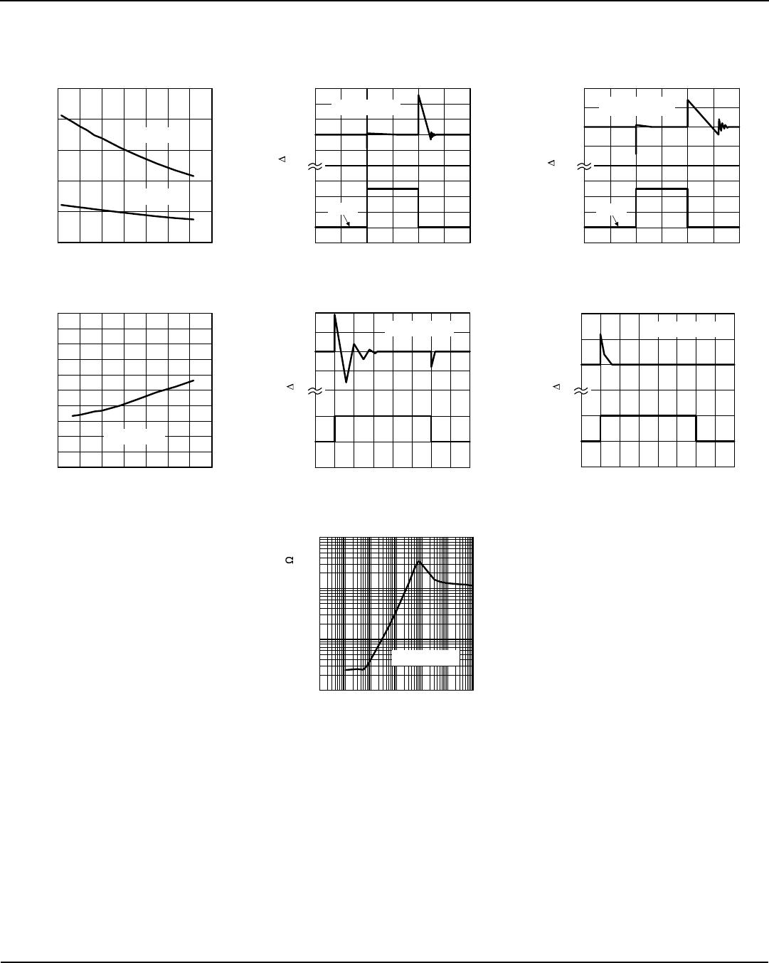
Typical Characteristics
0
100
200
300
400
500
0.00 0.25 0.50 0.75 1.00 1.25
DROPOUT VOLTAGE (mV)
OUTPUT CURRENT (A)
Dropout Voltage
vs. Output Current
0
200
400
600
800
1000
-60 -30 0 30 60 90 120 150
DROPOUT VOLTAGE (mV)
TEMPERATURE (°C)
Dropout Voltage
vs. Temperature
I
LOAD
= 1.25A
0
1
2
3
4
5
6
0123456
OUTPUT VOLTAGE (V)
INPUT VOLTAGE (V)
Dropout
Characteristics
I
LOAD
=5mA
I
LOAD
= 1.25A
0.1
1
10
40
11 0 100 1000 10000
GROUND CURRENT (mA)
OUTPUT CURRENT (mA)
Ground Current
vs. Output Current
10A
0
100
200
300
400
01234567 8
GROUND CURRENT (µA)
SUPPLY VOLTAGE (V)
Ground Current
vs. Supply Voltage
FIXED 5V
I
LOAD
=5mA
0
10
20
30
40
50
0246810
GROUND CURRENT (mA)
INPUT VOLTAGE (V)
Ground Current
vs. Supply Voltage
FIXED 3.3V DEVICE
I
LOAD
=1.25A
0.00
0.10
0.20
0.30
0.40
-60 -30 0 30 60 90 120 150
GROUND CURRENT (mA)
TEMPERATURE (°C)
Ground Current
vs. Temperature
I
LOAD
=5mA
0.0
0.2
0.4
0.6
0.8
1.0
1.2
1.4
1.6
1.8
2.0
-60 -30 0 30 60 90 120 150
GROUND CURRENT (mA)
TEMPERATURE (°C)
Ground Current
vs. Temperature
I
LOAD
=100mA
0
10
20
30
40
50
-60 -30 0 30 60 90 120 150
GROUND CURRENT (mA)
TEMPERATURE (°C)
Ground Current
vs. Temperature
I
LOAD
=1.25A
I
LOAD
= 100mA
3.20
3.22
3.24
3.26
3.28
3.30
3.32
3.34
3.36
3.38
3.40
-60 -30 0 30 60 90 120 150
OUTPUT VOLTAGE (V)
TEMPERATURE (°C)
Fixed 3.3V Output Voltage
vs. Temperature
0.0
0.2
0.4
0.6
0.8
1.0
1.2
1.4
1.6
1.8
2.0
-60 -30 0 30 60 90 120 150
CURRENT (A)
TEMPERATURE (°C)
Short Circuit and Maximum
Current vs. Temperature
V
OUT
=V
NOMINAL
–0.5V
V
OUT
=0V
FIXED 3.3V
VERSION
3SAMPLES
-200
0
200
400
600
800
1000
-30 -20 -10 0 10 20 30
GROUND CURRENT (µA)
INPUT VOLTAGE (V)
Ground Current
vs. Input Voltage
R
LOAD
= 100
Micrel, Inc. MIC2940A/2941A
July 2007
6
M9999-071307
Typical Characteristics (continued)
0
25
50
75
100
125
-60 -30 0 30 60 90 120 150
ENABLE CURRENT (µA)
TEMPERATURE (°C)
MIC29401/2 Shutdown Current
vs. Temperature
V
EN
=5V
V
EN
=2V
-500
-250
0
250
500
750
OUTPUT (mV)
-0.5
0.0
0.5
1.0
1.5
2.0
-5 0510
OUTPUT (A)
TIME (ms)
Load Transient
C
OUT
=1F
5mA
-200
-100
0
100
200
OUTPUT (mV)
-0.5
0.0
0.5
1.0
1.5
2.0
-5 0510
OUTPUT (A)
TIME (ms)
Load Transient
C
OUT
= 100 µF
5mA
0
10
20
30
40
50
-60 -30 0 30 60 90 120 150
ADJUST PIN CURRENT (nA)
TEMPERATURE (°C)
MIC29402/3 Adjust Pin
Current vs. Temperature
I
LOAD
=5mA
-40
-20
0
20
40
OUTPUT (mV)
4
6
8
10
-0.2 0.0 0.2 0.4 0.6 0.8 1.0 1.2 1.4
INPUT (V)
TIME (ms)
Line Transient
C
OUT
=1F
-10
0
10
20
OUTPUT (mV)
4
6
8
10
-0.2 0.0 0.2 0.4 0.6 0.8 1.0 1.2 1.4
INPUT (V)
TIME (ms)
Line Transient
C
OUT
= 100 µF
0.01
0.1
1
10
1x10
0
10x10
0
100x10
0
1x10
3
10x10
3
100x10
3
1x10
6
OUTPUT IMPEDANCE ( )
FREQUENCY (Hz)
Output Impedance
vs. Frequency
I
LOAD
= 10mA

MIC2941AWU

Mfr. #:
Manufacturer:
Microchip Technology / Micrel
Description:
LDO Voltage Regulators 1.25A LDO Adj+Shutdown
Lifecycle:
New from this manufacturer.
Delivery:
DHL FedEx Ups TNT EMS
Payment:
T/T Paypal Visa MoneyGram Western Union