AD7621
Rev. 0 | Page 6 of 32
Parameter Symbol Min Typ Max Unit
SLAVE SERIAL INTERFACE MODES
5
(Refer to Figure 40 and Figure 41)
External SCLK Setup Time t
31
5 ns
External SCLK Active Edge to SDOUT Delay t
32
1 8 ns
SDIN Setup Time t
33
5 ns
SDIN Hold Time t
34
5 ns
External SCLK Period t
35
12.5 ns
External SCLK High t
36
5 ns
External SCLK Low t
37
5 ns
1
See the Conversion Control section.
2
All timings for wideband warp mode are the same as warp mode.
3
In warp mode only, the time between conversions is 1 ms; otherwise, there is no required maximum time.
4
See the Digital Interface, and RESET sections.
5
In serial interface modes, the SYNC, SCLK, and SDOUT timings are defined with a maximum load C
L
of 10 pF; otherwise, the load is 60 pF maximum.
6
In serial master read during convert mode. See Table 4 for serial master read after convert mode timing specifications.
SERIAL CLOCK TIMING SPECIFICATIONS
Table 4. Serial Clock Timings in Master Read After Convert Mode
DIVSCLK[1] 0 0 1 1
DIVSCLK[0] Symbol 0 1 0 1 Unit
SYNC to SCLK First Edge Delay Minimum t
18
0.5 3 3 3 ns
Internal SCLK Period Minimum t
19
8 16 32 64 ns
Internal SCLK Period Maximum t
19
12 25 50 100 ns
Internal SCLK High Minimum t
20
2 6 15 31 ns
Internal SCLK Low Minimum t
21
3 7 16 32 ns
SDOUT Valid Setup Time Minimum t
22
1 5 5 5 ns
SDOUT Valid Hold Time Minimum t
23
0 0.5 10 28 ns
SCLK Last Edge to SYNC Delay Minimum t
24
0 0.5 9 26 ns
BUSY High Width Maximum (Wideband and Warp Modes) t
28
0.500 0.720 1.160 2.040 μs
BUSY High Width Maximum (Normal Mode) t
28
0.650 0.870 1.310 2.190 μs
BUSY High Width Maximum (Impulse Mode) t
28
0.780 1.000 1.440 2.320 μs
04565-002
NOTE
IN SERIAL INTERFACE MODES, THE SYNC, SCLK AND
SDOUT ARE DEFINED WITH A MAXIMUM LOAD.
C
L
OF 10pF; OTHERWISE, THE LOAD IS 60pF MAXIMUM.
500μAI
OL
500μAI
OH
1.4V
TO OUTPUT
PIN
C
L
50pF
Figure 2. Load Circuit for Digital Interface Timing,
SDOUT, SYNC, and SCLK Outputs, C
L
= 10 pF
0.8V
2V
2V
0.8V
0.8V
2V
t
DELAY
t
DELAY
05665-003
Figure 3. Voltage Reference Levels for Timing
AD7621
Rev. 0 | Page 7 of 32
ABSOLUTE MAXIMUM RATINGS
Table 5.
Parameter Rating
Analog Inputs/Outputs
IN+
1
, IN−, REF, REFBUFIN, TEMP,
INGND, REFGND to AGND
AVDD + 0.3 V to
AGND − 0.3 V
Ground Voltage Differences
AGND, DGND, OGND ±0.3 V
Supply Voltages
AVDD, DVDD –0.3 V to +2.7 V
OVDD –0.3 V to +3.8 V
AVDD to DVDD ±2.8 V
AVDD to OVDD +2.8 V to −3.8 V
OVDD to DVDD
2
≤ +0.3 V if DVDD < 2.3 V
Digital Inputs −0.3 V to +5.5 V
PDREF, PDBUF
3
±20 mA
Internal Power Dissipation
4
700 mW
Internal Power Dissipation
5
2.5 W
Junction Temperature 125°C
Storage Temperature Range –65°C to +125°C
1
See the Analog Inputs section.
2
See the Power Supply section.
3
See the Voltage Reference Input section.
4
Specification is for the device in free air: 48-Lead LQFP; θ
JA
= 91°C/W,
θ
JC
= 30°C/W.
5
Specification is for the device in free air: 48-Lead LFCSP; θ
JA
= 26°C/W.
Stresses above those listed under Absolute Maximum Ratings
may cause permanent damage to the device. This is a stress
rating only; functional operation of the device at these or any
other conditions above those indicated in the operational
section of this specification is not implied. Exposure to absolute
maximum rating conditions for extended periods may affect
device reliability.
ESD CAUTION
ESD (electrostatic discharge) sensitive device.
Charged devices and circuit boards can discharge
without detection. Although this product features
patented or proprietary protection circuitry, damage may
occur on devices subjected to high energy ESD.
Therefore, proper ESD precautions should be taken to
avoid
performance degradation or loss of functionality.
AD7621
Rev. 0 | Page 8 of 32
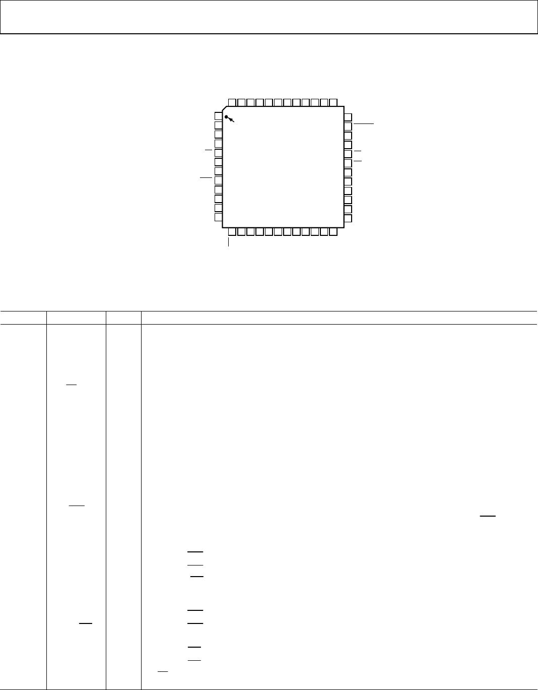
PIN CONFIGURATION AND FUNCTION DESCRIPTIONS
36
35
34
33
32
31
30
29
28
27
26
25
13 14 15 16 17 18 19 20 21 22 23 24
1
2
3
4
5
6
7
8
9
10
11
12
48 47 46 45 44 39 38 3743 42 41 40
PIN 1
IDENTIFIER
TOP VIEW
(Not to Scale)
AGND
CNVST
PD
RESET
CS
RD
DGND
AGND
AVDD
NC
BYTESWAP
OB/2C
NC = NO CONNECT
SER/PAR
D0
D1
D2/DIVSCLK[0]
BUSY
D15
D14
D13
AD7621
D3/DIVSCLK[1]
D12
D4/EXT/INT
D5/INVSYNC
D6/INVSCLK
D7/RDC/SDIN
OGND
OVDD
DVDD
DGND
D8/SDOUT
D9/SCLK
D10/SYNC
D11/RDERROR
PDBUF
PDREF
REFBUFIN
TEMP
AVDD
IN+
AGND
AGND
NC
IN–
REFGND
REF
IMPULSE
WARP
04565-004
Figure 4. Pin Configuration
Table 6. Pin Function Descriptions
Pin No. Mnemonic Type
1
Description
1, 41, 42 AGND P Analog Power Ground Pin.
2, 44 AVDD P Input Analog Power Pins. Nominally 2.5 V.
3, 40 NC No Connect.
4 BYTESWAP DI
Parallel Mode Selection (8-Bit/16-Bit). When high, the LSB is output on D[15:8] and the MSB is output
on D[7:0]; when low, the LSB is output on D[7:0] and the MSB is output on D[15:8].
5
OB/
2C
DI
Straight Binary/Binary Twos Complement Output. When high, the digital output is straight binary;
when low, the MSB is inverted resulting in a twos complement output from its internal shift register.
6 WARP DI
Conversion Mode Selection. When WARP = high and IMPULSE = high, this selects wideband mode
with slightly improved linearity and THD. When WARP = high and IMPULSE = low, this selects warp
mode. In either mode, these are the fastest modes; maximum throughput is achievable, and a
minimum conversion rate must be applied in order to guarantee full specified accuracy.
When WARP = low and IMPULSE = low, this input selects normal mode where full accuracy is
maintained independent of the minimum conversion rate.
7 IMPULSE DI
Conversion Mode Selection. When IMPULSE = high and WARP = low, this input selects impulse mode,
a reduced power mode. In this mode, the power dissipation is approximately proportional to the
sampling rate.
8
SER/
PAR
DI
Serial/Parallel Selection Input. When high, the serial interface is selected and some bits of the data bus
are used as a serial port; the remaining data bits are high impedance outputs. When SER/
PAR = low,
the parallel port is selected.
9, 10 D[0:1] DO Bit 0 and Bit 1 of the Parallel Port Data Output Bus.
11, 12 D[2:3] DI/O
When SER/
PAR = low, these outputs are used as Bit 2 and Bit 3 of the parallel port data output bus.
or
DIVSCLK[0:1]
When SER/
PAR = high, serial clock division selection. When using serial master read after convert
mode (EXT/
INT = low, RDC/SDIN = low) these inputs can be used to slow down the internally
generated serial clock that clocks the data output. In other serial modes, these pins are high
impedance outputs.
13 D4 DI/O
When SER/
PAR = low, this output is used as Bit 4 of the parallel port data output bus.
or EXT/
INT
When SER/
PAR = high, serial clock source select. This input is used to select the internally generated
(master ) or external (slave) serial data clock.
When EXT/
INT = low: master mode. The internal serial clock is selected on SCLK output.
When EXT/
INT = high: slave mode. The output data is synchronized to an external clock signal, gated
by CS, connected to the SCLK input.

AD7621ASTZRL

Mfr. #:
Manufacturer:
Analog Devices Inc.
Description:
Analog to Digital Converters - ADC 16B 2LSB INL 3 MSPS
Lifecycle:
New from this manufacturer.
Delivery:
DHL FedEx Ups TNT EMS
Payment:
T/T Paypal Visa MoneyGram Western Union

Products related to this Datasheet