ZXM61P03F
SEMICONDUCTORS
ISSUE 1 - OCTOBER 2005
4
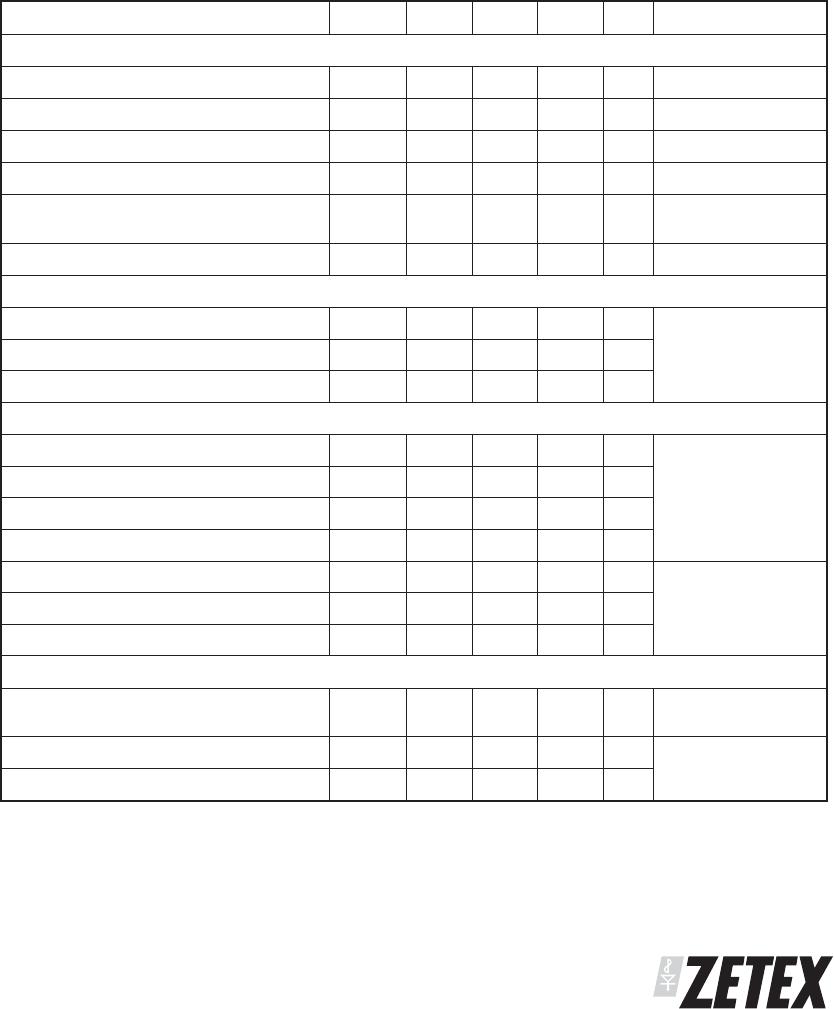
ELECTRICAL CHARACTERISTICS (at T
amb
= 25°C unless otherwise stated).
PARAMETER SYMBOL MIN. TYP. MAX. UNIT CONDITIONS.
STATIC
Drain-Source Breakdown Voltage V
(BR)DSS
-30 V
I
D
=-250µA, V
GS
=0V
Zero Gate Voltage Drain Current I
DSS
-1
µA
V
DS
=-30V, V
GS
=0V
Gate-Body Leakage I
GSS
⫾100
nA V
GS
=⫾20V, V
DS
=0V
Gate-Source Threshold Voltage V
GS(th)
-1.0 V
I
D
=-250µA, V
DS
=V
GS
Static Drain-Source On-State Resistance (1) R
DS(on)
0.35
0.55
Ω
Ω
V
GS
=-10V, I
D
=-0.6A
V
GS
=-4.5V, I
D
=-0.3A
Forward Transconductance (3) g
fs
0.44 S V
DS
=-10V,I
D
=-0.3A
DYNAMIC (3)
Input Capacitance C
iss
140 pF
V
DS
=-25 V, V
GS
=0V,
f=1MHz
Output Capacitance C
oss
45 pF
Reverse Transfer Capacitance C
rss
20 pF
SWITCHING(2) (3)
Turn-On Delay Time t
d(on)
1.9 ns
V
DD
=-15V, I
D
=-0.6A
R
G
=6.2Ω,R
D
=25Ω
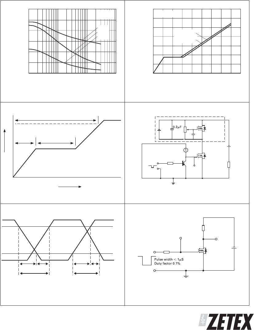
(Refer to test circuit)
Rise Time t
r
2.9 ns
Turn-Off Delay Time t
d(off)
8.9 ns
Fall Time t
f
5.0 ns
Total Gate Charge Q
g
4.8 nC
V
DS
=-24V,V
GS
=-10V,
I
D
=-0.6A
(Refer to test circuit)
Gate-Source Charge Q
gs
0.62 nC
Gate Drain Charge Q
gd
1.3 nC
SOURCE-DRAIN DIODE
Diode Forward Voltage (1) V
SD
-0.95 V T
j
=25°C, I
S
=-0.6A,
V
GS
=0V
Reverse Recovery Time (3) t
rr
14.8 ns T
j
=25°C, I
F
=-0.6A,
di/dt= 100A/µs
Reverse Recovery Charge(3) Q
rr
7.7 nC
NOTES:
(1) Measured under pulsed conditions. Width=300µs. Duty cycle ⱕ2%.
(2) Switching characteristics are independent of operating junction temperature.
(3) For design aid only, not subject to production testing.