L4949ED-E, L4949EP-E Application information
Doc ID 16823 Rev 2 13/19
3.5 Reset circuit
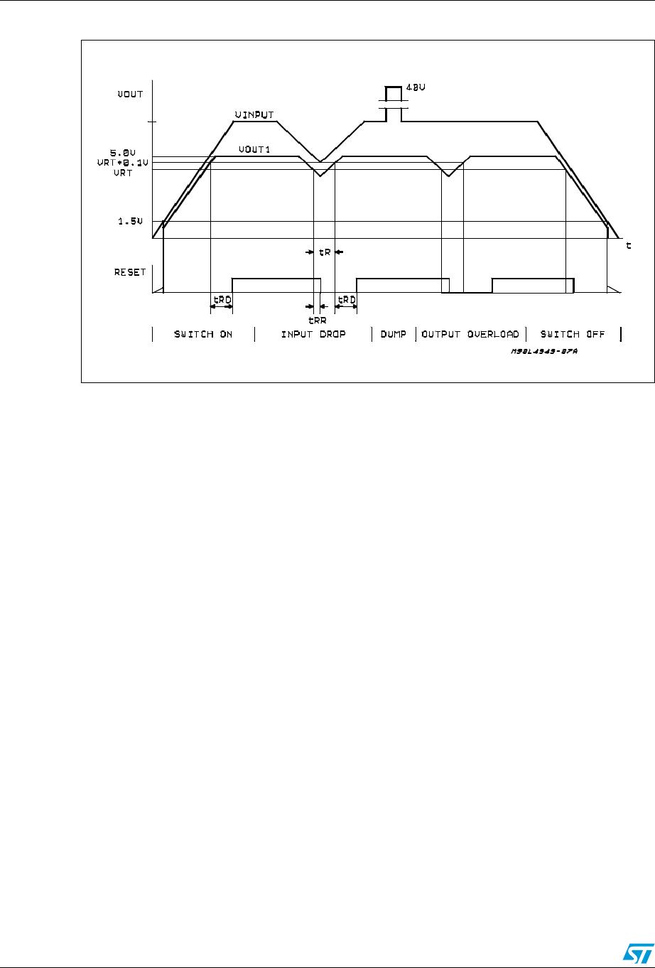
The block circuit diagram of the reset circuit is shown in Figure 7. The reset circuit
supervises the output voltage.
The reset threshold of 4.5 V is defined with the internal reference voltage and standby
output divider.
The reset pulse delay time t
RD
, is defined with the charge time of an external capacitor C
T
:
The reaction time of the reset circuit originates from the discharge time limitation of the reset
capacitor CT and is proportional to the value of CT.
The reaction time of the reset circuit increases the noise immunity. Standby output voltage
drops below the reset threshold only a bit longer than the reaction time results in a shorter
reset delay time.
The nominal reset delay time is generated for standby output voltage drops longer than
approximately 50ms.
The typical reset output waveforms are shown in Figure 8.
3.6 Sense comparator
The sense comparator compares an input signal with an internal voltage reference of typical
1.23V. The use of an external voltage divider makes this comparator very flexible in the
application.
It can be used to supervise the input voltage either before or after the protection diode and
to give additional informations to the microprocessor like low voltage warnings.
Figure 7. Block circuit of reset circuit
t
RD
C
T
2V•
2μA
-------------------- -=