List of figures L4949ED-E, L4949EP-E
4/19 Doc ID 16823 Rev 2
List of figures
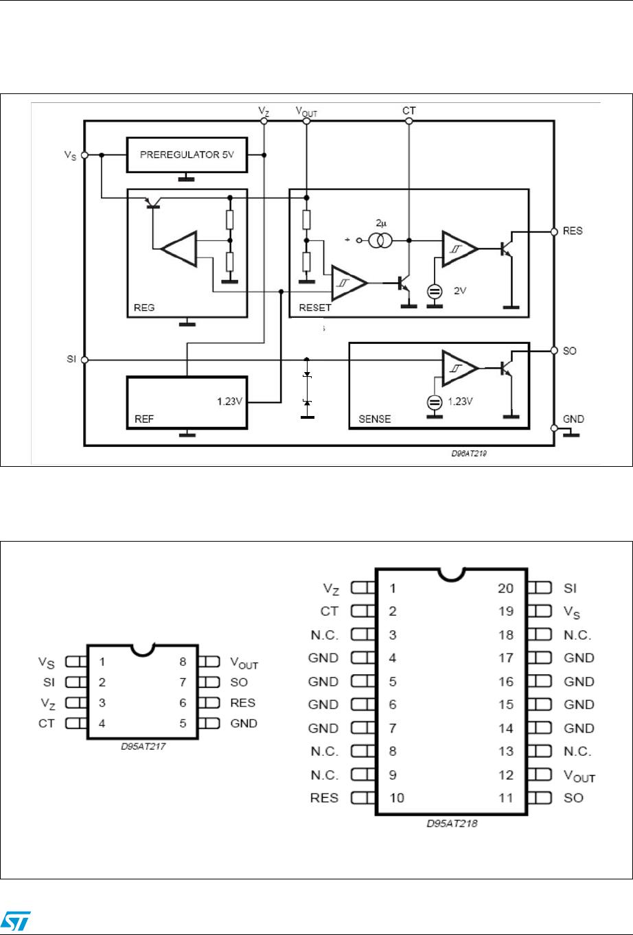
Figure 1. Block diagram. . . . . . . . . . . . . . . . . . . . . . . . . . . . . . . . . . . . . . . . . . . . . . . . . . . . . . . . . . . . 5
Figure 2. Configuration diagram (top view) . . . . . . . . . . . . . . . . . . . . . . . . . . . . . . . . . . . . . . . . . . . . . 5
Figure 3. Application circuit
(1)
. . . . . . . . . . . . . . . . . . . . . . . . . . . . . . . . . . . . . . . . . . . . . . . . . . . . . . 10
Figure 4. Foldback characteristic of V
O
. . . . . . . . . . . . . . . . . . . . . . . . . . . . . . . . . . . . . . . . . . . . . . . 11
Figure 5. Output voltage vs input voltage . . . . . . . . . . . . . . . . . . . . . . . . . . . . . . . . . . . . . . . . . . . . . 12
Figure 6. Quiescent current vs supply voltage. . . . . . . . . . . . . . . . . . . . . . . . . . . . . . . . . . . . . . . . . . 12
Figure 7. Block circuit of reset circuit . . . . . . . . . . . . . . . . . . . . . . . . . . . . . . . . . . . . . . . . . . . . . . . . . 13
Figure 8. Waveforms . . . . . . . . . . . . . . . . . . . . . . . . . . . . . . . . . . . . . . . . . . . . . . . . . . . . . . . . . . . . . 14
Figure 9. SO-8 TP package dimensions . . . . . . . . . . . . . . . . . . . . . . . . . . . . . . . . . . . . . . . . . . . . . . 16
Figure 10. SO20 TP package dimensions . . . . . . . . . . . . . . . . . . . . . . . . . . . . . . . . . . . . . . . . . . . . . . 17
L4949ED-E, L4949EP-E Block diagram and pin description
Doc ID 16823 Rev 2 5/19
1 Block diagram and pin description
Figure 1. Block diagram
Note: The block diagram illustrates only a major internal device functionality and it is not intended
to mimic any details of hardware design
Figure 2. Configuration diagram (top view)
SO-8
SO-20
Block diagram and pin description L4949ED-E, L4949EP-E
6/19 Doc ID 16823 Rev 2
Table 2. Pin definitions and functions
Pin N°
Symbol Function
SO-8 SO-20
119 V
S
Input supply voltage. Block to GND via an external
capacitor (see Figure 3).
220 S
I
Sense input pin to supervise input voltage. Connect via an
external voltage divider connected to V
S
and to GND.
31 V
Z
Preregulator output voltage. For details, see Section 3.4:
Preregulator.
42 C
T
Reset pulse delay adjustment. Connecting this pin via a
capacitor to GND
5
4, 5, 6, 7, 14,
15, 16, 17
GND Ground reference
610 RES
Reset output. It is pulled down when the output voltage
goes below V
RT
.
711 S
O
Sense output. This open collector pin must be connected to
V
OUT
via an external resistor. It is pulled down whenever
the S
I
voltage becomes lower than an internal voltage.
812 V
OUT
Output voltage. Block to GND via an external capacitor (see
Figure 3)
- 3, 8, 9, 13, 18 NC Not connected pins

L4949EDTR-E

Mfr. #:
Manufacturer:
STMicroelectronics
Description:
LDO Voltage Regulators 5V MULTIFUNCTION LDO
Lifecycle:
New from this manufacturer.
Delivery:
DHL FedEx Ups TNT EMS
Payment:
T/T Paypal Visa MoneyGram Western Union

Products related to this Datasheet