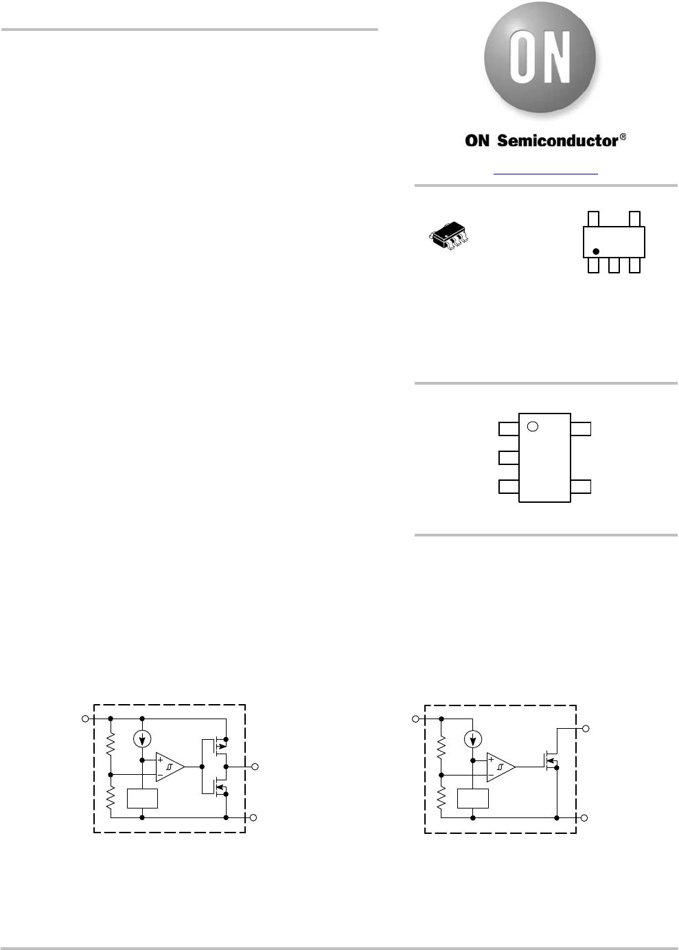
© Semiconductor Components Industries, LLC, 2016
May, 2016 − Rev. 29
1 Publication Order Number:
NCP300/D
NCP300, NCP301
Voltage Detector Series
The NCP300 and NCP301 series are second generation ultra−low
current voltage detectors. These devices are specifically designed for
use as reset controllers in portable microprocessor based systems
where extended battery life is paramount.
Each series features a highly accurate undervoltage detector with
hysteresis which prevents erratic system reset operation as the
comparator threshold is crossed.
The NCP300 series consists of complementary output devices that
are available with either an active high or active low reset output. The
NCP301 series has an open drain N−Channel output with either an
active high or active low reset output.
The NCP300 and NCP301 device series are available in the
Thin TSOP−5 package with standard undervoltage thresholds.
Additional thresholds that range from 0.9 V to 4.9 V in 100 mV steps
can be manufactured.
Features
Quiescent Current of 0.5 mA Typical
High Accuracy Undervoltage Threshold of 2.0%
Wide Operating Voltage Range of 0.8 V to 10 V
Complementary or Open Drain Reset Output
Active Low or Active High Reset Output
Specified Over the −40°C to +125°C Temperature Range
(Except for Voltage Options from 0.9 to 1.1 V)
NCV Prefix for Automotive and Other Applications Requiring
Unique Site and Control Change Requirements; AEC−Q100
Qualified and PPAP Capable
These Devices are Pb−Free and are RoHS Compliant
Typical Applications
Microprocessor Reset Controller
Low Battery Detection
Power Fail Indicator
Battery Backup Detection
Figure 1. Representative Block Diagrams
This device contains 25 active transistors.
NCP301xSNxxT1
Open Drain Output Configuration
NCP300xSNxxT1
Complementary Output Configuration
V
ref
V
ref
Input
Reset Output
GND
3
1
2
Input
Reset Output
GND
3
1
2
*
*
* The representative block diagrams depict active low reset output ‘L’ suffix devices. The comparator
inputs are interchanged for the active high output ‘H’ suffix devices.
See detailed ordering and shipping information in the ordering
information section on page 21 of this data sheet.
ORDERING INFORMATION
1
5
www.onsemi.com
TSOP−5/
SOT23−5
CASE 483
PIN CONNECTIONS
1
3
N.C.
Reset
Output
2
Input
Ground
4
N.C.
5
(Top View)
1
5
xxx AYWG
G
MARKING DIAGRAM
xxx = Specific Device Code
A = Assembly Location
Y = Year
W = Work Week
G = Pb−Free Package
(Note:Microdot may be in either location)
NCP300, NCP301
www.onsemi.com
2
MAXIMUM RATINGS
Rating Symbol Value Unit
Input Power Supply Voltage (Pin 2) V
in
12 V
Output Voltage (Pin 1)
Complementary, NCP300
N−Channel Open Drain, NCP301
V
OUT
−0.3 to V
in
+0.3
−0.3 to 12
V
Output Current (Pin 1) (Note 2) I
OUT
70 mA
Thermal Resistance Junction−to−Air
R
q
JA
250 °C/W
Maximum Junction Temperature T
J
+150 °C
Operating Ambient Temperature Range
All Voltage Options: 0.9 V to 1.1 V
All Voltage Options: 1.2 V to 4.9 V
T
A
T
A
−40 to +85
−40 to +125
°C
°C
Storage Temperature Range T
stg
−55 to +150 °C
Moisture Sensitivity Level MSL 1
Latchup Performance (Note 3)
Positive
Negative
I
LATCHUP
200
200
mA
Stresses exceeding those listed in the Maximum Ratings table may damage the device. If any of these limits are exceeded, device functionality
should not be assumed, damage may occur and reliability may be affected.
1. This device series contains ESD protection and exceeds the following tests:
Human Body Model 2000 V per MIL−STD−883, Method 3015.
Machine Model Method 200 V.
2. The maximum package power dissipation limit must not be exceeded.
P
D
+
T
J(max)
* T
A
R
qJA
3. Maximum ratings per JEDEC standard JESD78.
NCP300, NCP301
www.onsemi.com
3
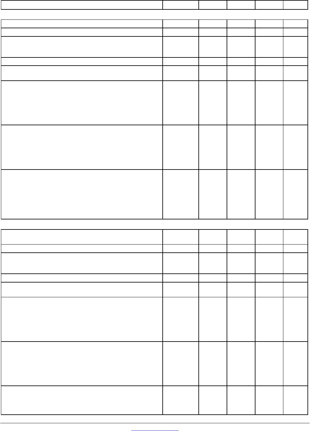
ELECTRICAL CHARACTERISTICS (For all values T
A
= −40°C to +125°C, unless otherwise noted.)
Characteristic
Symbol Min Typ Max Unit
NCP300/1 − 0.9 / NCV300/1 − 0.9 (T
A
= 255C for voltage options from 0.9 to 1.1 V)
Detector Threshold (Pin 2, V
in
Decreasing) V
DET−
0.882 0.900 0.918 V
Detector Threshold Hysteresis (Pin 2, V
in
Increasing) V
HYS
0.027 0.045 0.063 V
Supply Current (Pin 2)
(V
in
= 0.8 V)
(V
in
= 2.9 V)
I
in
0.20
0.45
0.6
1.2
mA
Maximum Operating Voltage (Pin 2) V
in(max)
10 V
Minimum Operating Voltage (Pin 2)
(T
A
= −40°C to 85°C)
V
in(min)
0.55
0.65
0.70
0.80
V
Reset Output Current (Pin 1, Active Low ‘L’ Suffix Devices) I
OUT
mA
N−Channel Sink Current, NCP300, NCP301
(V
OUT
= 0.05 V, V
in
= 0.70 V)
(V
OUT
= 0.50 V, V
in
= 0.85 V)
0.01
0.05
0.05
0.50
P−Channel Source Current, NCP300
(V
OUT
= 2.4 V, V
in
= 4.5 V)
1.0 6.0
Reset Output Current (Pin 1, Active High ‘H’ Suffix Devices) I
OUT
mA
N−Channel Sink Current, NCP300, NCP301
(V
OUT
= 0.5 V, V
in
= 1.5 V)
1.05 2.5
P−Channel Source Current, NCP300
(V
OUT
= 0.4 V, V
in
= 0.7 V)
(V
OUT
= GND, V
in
= 0.8 V)
0.011
0.014
0.04
0.08
Propagation Delay Input to Output (Figure 2)
ms
Complementary Output NCP300 Series
Output Transition, High to Low
Output Transition, Low to High
t
pHL
t
pLH
97
77
300
N−Channel Open Drain NCP301 Series
Output Transition, High to Low
Output Transition, Low to High
t
pHL
t
pLH
97
300
NCP300/1 − 1.8 / NCV300/1 − 1.8
Detector Threshold (Pin 2, V
in
Decreasing) (T
A
= 25°C)
(T
A
= −40°C to 125°C)
V
DET−
1.764
1.746
1.80
1.836
1.854
V
Detector Threshold Hysteresis (Pin 2, V
in
Increasing) V
HYS
0.054 0.090 0.126 V
Supply Current (Pin 2)
(V
in
= 1.7 V)
(V
in
= 3.8 V)
I
in
0.23
0.48
0.7
1.3
mA
Maximum Operating Voltage (Pin 2) V
in(max)
10 V
Minimum Operating Voltage (Pin 2) (T
A
= 25°C)
(T
A
= −40°C to 125°C)
V
in(min)
0.55
0.65
0.70
0.80
V
Reset Output Current (Pin 1, Active Low ‘L’ Suffix Devices) I
OUT
mA
N−Channel Sink Current, NCP300, NCP301
(V
OUT
= 0.05V, V
in
= 0.70 V)
(V
OUT
= 0.50V, V
in
= 1.5 V)
0.01
1.0
0.05
2.0
P−Channel Source Current, NCP300
(V
OUT
= 2.4 V, V
in
= 4.5 V)
1.0 6.0
Reset Output Current (Pin 1, Active High ‘H’ Suffix Devices) I
OUT
mA
N−Channel Sink Current, NCP300, NCP301
(V
OUT
= 0.5 V, V
in
= 5.0 V)
6.3 11
P−Channel Source Current, NCP300
(V
OUT
= 0.4 V, V
in
= 0.7 V)
(V
OUT
= GND, V
in
= 1.5 V)
0.011
0.525
0.04
0.6
Propagation Delay Input to Output (Figure 2)
ms
Complementary Output NCP300 Series
Output Transition, High to Low
Output Transition, Low to High
t
pHL
t
pLH
73
94
300

NCP300LSN28T1G

Mfr. #:
Manufacturer:
ON Semiconductor
Description:
Supervisory Circuits 2.8V Detector w/Reset Low
Lifecycle:
New from this manufacturer.
Delivery:
DHL FedEx Ups TNT EMS
Payment:
T/T Paypal Visa MoneyGram Western Union