NCP300, NCP301
www.onsemi.com
21
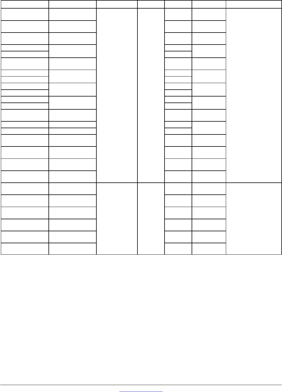
ORDERING INFORMATION
Device Threshold Voltage Output Type Reset Marking Package Shipping
†
NCP300LSN09T1G 0.9
CMOS
Active
Low
SEJ TSOP−5
(Pb−Free)
3000 / Tape & Reel
(7 in. Reel)
NCP300LSN18T1G 1.8 SFK TSOP−5
(Pb−Free)
NCP300LSN185T1G 1.85 SRA TSOP−5
(Pb−Free)
NCP300LSN20T1G
2.0
SHE
TSOP−5
(Pb−Free)
NCV300LSN20T1G* SIM
NCP300LSN25T1G 2.5
RUM
TSOP−5
(Pb−Free)
NCP300LSN27T1G
2.7
SEE
TSOP−5
(Pb−Free)
NCV300LSN27T1G* SIW
NCP300LSN28T1G
2.8
SED
TSOP−5
(Pb−Free)
NCV300LSN28T1G* SSL
NCP300LSN30T1G
3.0
SEC
TSOP−5
(Pb−Free)
NCV300LSN30T1G* SQV
NCP300LSN33T1G 3.3 SKV TSOP−5
(Pb−Free)
NCP300LSN34T1G 3.4 SKU
TSOP−5
(Pb−Free)
NCV300LSN36T1G* 3.6 SKS
NCP300LSN44T1G 4.4 SKK TSOP−5
(Pb−Free)
NCP300LSN45T1G 4.5 SEA TSOP−5
(Pb−Free)
NCP300LSN46T1G 4.6 SKJ TSOP−5
(Pb−Free)
NCP300LSN47T1G 4.7 SDZ TSOP−5
(Pb−Free)
NCP300HSN09T1G 0.9
CMOS
Active
High
SDY TSOP−5
(Pb−Free)
3000 / Tape & Reel
(7 in. Reel)
NCP300HSN18T1G 1.8 SFJ TSOP−5
(Pb−Free)
NCP300HSN27T1G 2.7 SDU TSOP−5
(Pb−Free)
NCP300HSN30T1G 3.0 SDS TSOP−5
(Pb−Free)
NCP300HSN45T1G 4.5 SDQ TSOP−5
(Pb−Free)
NCP300HSN47T1G 4.7 SDP TSOP−5
(Pb−Free)
NOTE: The ordering information lists standard undervoltage thresholds with active low outputs. Additional active low threshold devices,
ranging from 0.9 V to 4.9 V in 100 mV increments and NCP300/NCP301 active high output devices, ranging from 0.9 V to 4.9 V
in 100 mV increments can be manufactured. Contact your ON Semiconductor representative for availability. The electrical
characteristics of these additional devices are shown in Tables 1 through 4.
†For information on tape and reel specifications, including part orientation and tape sizes, please refer to our Tape and Reel Packaging Spe-
cifications Brochure, BRD8011/D.
*NCV prefix for Automotive and Other Applications Requiring Unique Site and Control Change Requirements; AEC−Q100 Qualified and PPAP
Capable.
NCVxxx: T
low
= −40°C, T
high
= +125°C. Guaranteed by design.