NCP300, NCP301
www.onsemi.com
13
Figure 15. NCP300L Series 0.9 V
Reset Output Source Current versus Input Voltage
Figure 16. NCP300L Series 2.7 V
Reset Output Source Current versus Input Voltag
e
Figure 17. NCP300L Series 4.5 V
Reset Output Source Current versus Input Voltage
Figure 18. NCP300H/1L Series 0.9 V
Reset Output Sink Current versus Output Voltage
Figure 19. NCP300H/1L Series 2.7 V
Reset Output Sink Current versus Output Voltage
Figure 20. NCP300H/1L Series 4.5 V
Reset Output Sink Current versus Output Voltage
0
35
25
15
5.0
1.0
2.0 3.0
10
0
4
.0
20
30
V
OUT
, OUTPUT VOLTAGE (V)
T
A
= 25°C
V
in
= 4.0 V
V
in
= 3.5 V
V
in
= 3.0 V
V
in
= 2.5 V
V
in
= 2.0 V
V
in
= 1.5 V
I
OUT
, OUTPUT SINK CURRENT (mA)
I
OUT
, OUTPUT SOURCE CURRENT (mA)
15
0
0
2.0
4.0
6.0
8.0
10
V
in
, INPUT VOLTAGE (V)
5.0
10
20
V
OUT
= V
in
−2.1 V
T
A
= 25°C
V
in
−1.5 V
V
in
−1.0 V
V
in
−0.5 V
I
OUT
, OUTPUT SINK CURRENT (mA)
15
10
5.0
0
0
0.5
1.0
1.5 2.0
2.5
V
OUT
, OUTPUT VOLTAGE (V)
V
in
= 2.5 V
V
in
= 2.0 V
V
in
= 1.5 V
T
A
= 25°C
I
OUT
, OUTPUT SOURCE CURRENT (mA)
15
0
0
2.0
4.0
6.0
8.0
1
0
V
in
, INPUT VOLTAGE (V)
5.0
10
20
V
OUT
= V
in
−2.1 V
V
in
−1.5 V
V
in
−1.0 V
V
in
−0.5 V
T
A
= 25°C
20
5.0
0
0
2.0 4.0 6.0
8.0
10
V
in
, INPUT VOLTAGE (V)
10
15
V
OUT
= V
in
−2.1 V
V
in
−1.5 V
V
in
−1.0 V
V
in
−0.5 V
T
A
= 25°C
I
OUT
, OUTPUT SOURCE CURRENT (mA)
I
OUT
, OUTPUT SINK CURRENT (mA)
0
V
OUT
, OUTPUT VOLTAGE (V)
0.2
0.4
0.6 0.8
1
.0
1.5
0.5
0
1.0
V
in
= 0.85 V
T
A
= 25°C
V
in
= 0.7 V
NCP300, NCP301
www.onsemi.com
14
OPERATING DESCRIPTION
The NCP300 and NCP301 series devices are second
generation ultra−low current voltage detectors. Figures 20
and 21 show a timing diagram and a typical application.
Initially consider that input voltage V
in
is at a nominal level
and it is greater than the voltage detector upper threshold
(V
DET+
), and the reset output (Pin 1) will be in the high state
for active low devices, or in the low state for active high
devices. If there is a power interruption and V
in
becomes
significantly deficient, it will fall below the lower detector
threshold (V
DET−
). This sequence of events causes the Reset
output to be in the low state for active low devices, or in the
high state for active high devices. After completion of the
power interruption, V
in
will again return to its nominal level
and become greater than the V
DET+
. The voltage detector
has built−in hysteresis to prevent erratic reset operation as
the comparator threshold is crossed.
Although these device series are specifically designed for
use as reset controllers in portable microprocessor based
systems, they offer a cost−effective solution in numerous
applications where precise voltage monitoring is required.
Figure 26 through Figure 33 shows various application
examples.
Figure 21. Timing Waveforms
V
in
V
DET
+
V
DET−
Input Voltage, Pin 2
V
in
0 V
Reset Output (Active Low), Pin 1
Reset Output (Active High), Pin 1
V
in
0 V
V
DET
+
V
DET−
V
DET
+
V
DET−
NCP300, NCP301
www.onsemi.com
15
V
CC
TRANSIENT REJECTION
The NCP300 and NCP301 series provides accurate V
CC
monitoring and reset timing during power−up,
power−down, and brownout/sag conditions, and rejects
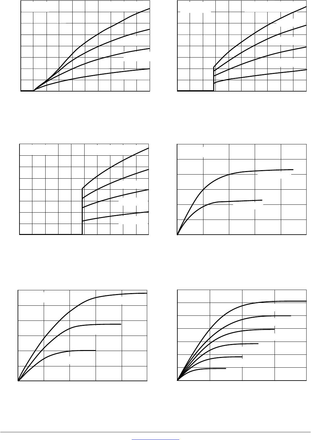
negative glitches on the power supply line. Figure 22 shows
the maximum transient duration vs. maximum negative
excursion (overdrive) for glitch rejection. Any combination
of duration and overdrive which lies under the curve will not
generate a reset signal. A below−V
CC
condition (on the
right) is detected as a brownout or power−down. Typically,
any transient that goes 100 mV below the reset threshold and
lasts 5.0 ms or less will not cause a reset pulse.
Transient immunity can be improved by adding a
capacitor in close proximity to the V
CC
pin of the NCP30x.
V
CC
V
TH
Duration
Overdrive
Figure 22. Max Transient Duration vs. Max Overdrive
Figure 23.
RESET COMPARATOR OVERDRIVE
TRANSIENT DURATION
300
250
200
150
100
50
0
1501301109070503010
V
TH
= 4.90 V
V
TH
= 3.10 V
V
TH
= 1.60 V
FACTORS TO BE CONSIDERED FOR VOLTAGE
OPTION SELECTION
The following hysteresis graph depicts V
DET−_min/max
and V
DET+_min/max
for an active low Reset device:
Output
Input
Figure 24.
V
DET−_min
V
DET−_max
V
DET+_min
V
DET+_max
V
DET−_typ
V
DET+_min
= V
DET−_min
+ V
HYS_min
V
DET+_max
= V
DET−_max
+ V
HYS_max
For selecting a voltage option in the NCP30X family,
three major factors should be considered:
1. V
DET+_max
: Maximum detector threshold voltage
for increasing V
in
for the NCP30X device.
2. V
in_min
: Minimum voltage output of the power
supply. This is also the input voltage to the
NCP30X device.
3. V
CC_min
: Minimum power supply voltage
specification for the device that is protected by the
NCP30X.
The V
DET+_max
for an NCP30X device is normally
calculated as follows:
V
DET+_max
+ V
DET−_max
) V
HYS_max
(eq. 1)
Where:
V
DET−_max
= Maximum detector threshold voltage for
decreasing Vin
V
HYS_max
= Maximum detector threshold hysteresis
The above two parameters can be obtained directly from
the data sheet to figure out the V
DET+_max
.
In the NCP30X family, for a given V
DET−_typ
, which is the
typical detection voltage reflected in the part number, the
threshold values are designed to the following targets (at
25°C):
V
DET−_min
+ V
DET−_typ
* 2%
(eq. 2)
V
DET−_max
+ V
DET−_typ
) 2%
(eq. 3)
V
HYS_typ
+ 5% of V
DET−_typ
(eq. 4)
V
HYS_min
+ V
HYS_typ
* 40%
(eq. 5)
V
HYS_max
+ V
HYS_typ
) 40%
(eq. 6)
By simple mathematical calculation, combining
Equations 2 to 6, Equation 1 becomes:
V
DET+_max
+ V
DET−_typ
1.09
(eq. 7)

NCP301HSN45T1G

Mfr. #:
Manufacturer:
ON Semiconductor
Description:
Supervisory Circuits 4.5V Detector w/Reset High
Lifecycle:
New from this manufacturer.
Delivery:
DHL FedEx Ups TNT EMS
Payment:
T/T Paypal Visa MoneyGram Western Union