NCP300, NCP301
www.onsemi.com
16
So, V
DET+_max
can be easily figured out just using a single
variable V
DET−_typ
.
For example, for NCP300LSN18T1G V
DET−_typ
= 1.8 V;
then
V
DET+_max
+ 1.8 1.09 + 1.962 V
(eq. 8)
The NCP30X detection voltage option must be chosen such
that:
V
CC_min
t V
DET+_max
t V
in_min
(eq. 9)
The significance of V
CC_min
< V
DET+_max
is that it makes
sure the the reset from NCP30X remains asserted (in RESET
hold state) till after the power supply exceeds the V
CC_min
requirement; this prevents incorrect device (uP) initiation.
Having V
DET+_max
< V
in_min
makes sure that the
NCP30X is able to start up when V
in
is at the V
in_min
.
The theoretical ideal V
DET−_typ
voltage option to be
selected by the user, V
DET−_typ_ideal
, can be given by the
following formula:
V
DET−_typ_ideal
+
ǒ
V
in_min
) V
CC_min
Ǔ
(
2 1.09
)
(eq. 10)
The following example shows how to select the device
voltage option in a real world application.
1. Power supply output specification: 3.3 V $3%
2. Microprocessor core voltage specification: 3.3 V
$5%
So, we have:
V
in_min
+ 3.3 V * 3% + 3.201 V
(eq. 11)
V
CC_min
+ 3.3 V * 5% + 3.135 V
(eq. 12)
Then the ideal voltage option = (3.201 + 3.135) / (2 * 1.09)
= 2.9064 V
Therefore, a device voltage option of 2.9 V will be the right
choice.
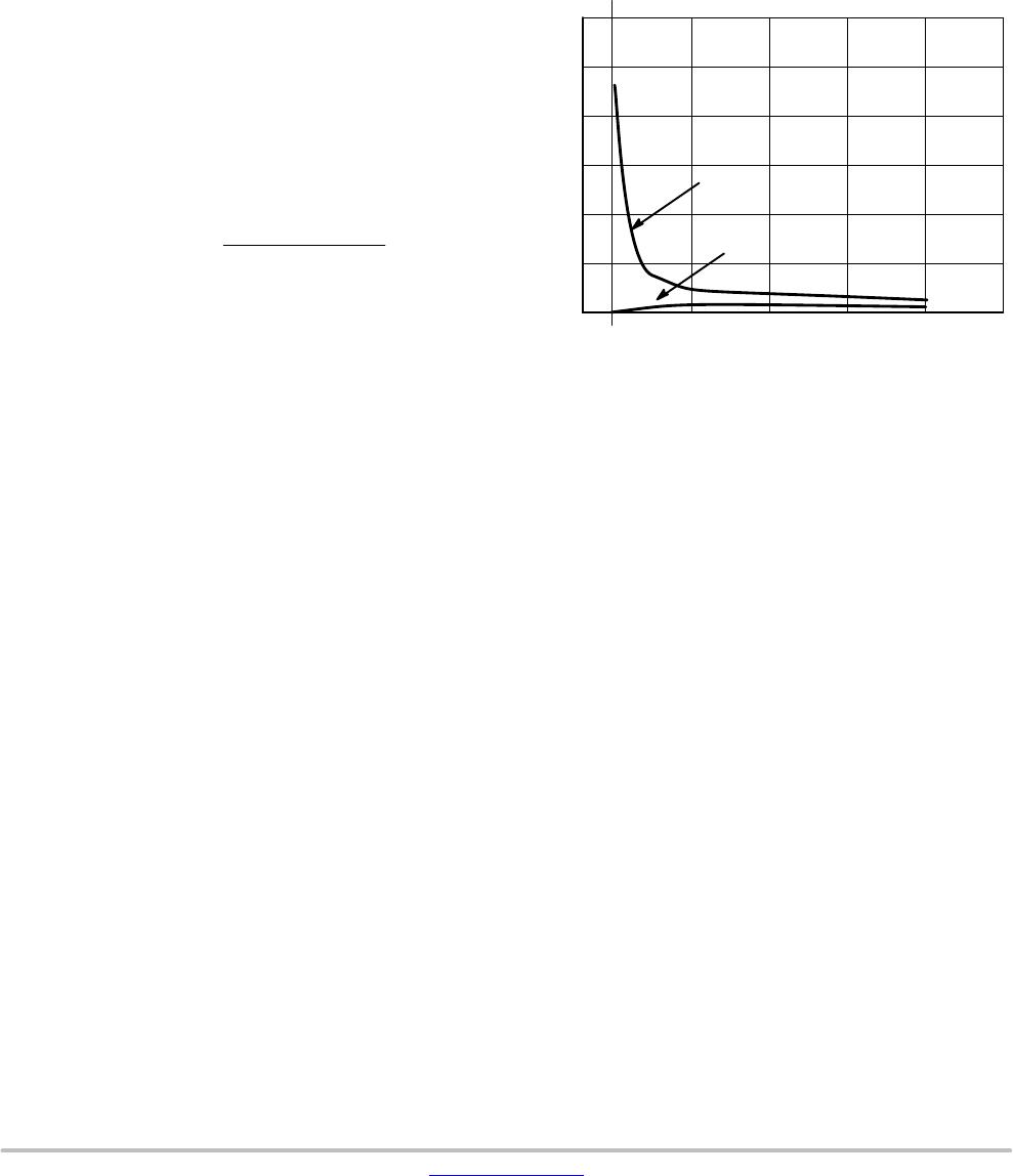
PROPAGATION DELAY VARIATION
On the other hand (see above paragraph), a minimum
overdrive value from V
threshold
to V
CC
must be respected.
That means V
in
(minimum value of V
CC
) must be higher
enough than V
DET+
(V
DET−
+ hysteresis) at the risk of
significantly increasing propagation delay. (Figure 25) This
propagation delay is temperature sensitive.
To avoid acceptable time response, a minimum 100 mV
difference between V
in
and V
DET+
must be selected.
Figure 25. t
pLH
and t
pHL
vs. Input Voltage
for the NCP301SNT1
t
pLH
t
pHL
5.0
4.54.03.5
5
.5
V
DET
+
TIME DELAY (ms)
100
0
300
200
500
400
600
3.0
3.168
V
in
, PULSE HIGH INPUT VOLTAGE (V)
NCP300, NCP301
www.onsemi.com
17
APPLICATION CIRCUIT INFORMATION
Figure 26. Microprocessor Reset Circuit
2 Input
1
Reset Output
GND
NCP300
LSN27T1
Figure 27. Battery Charge Indicator
2 Input
1
Reset Output
GND
GND
V
DD
Reset
V
DD
NCP300
Series
3
3
Microprocessor
* Required for
NCP301
V
in
< 2.7 ON
V
in
> 2.835 ON
To Additional Circuitry
*
2.85 V
2.70 V
Output
2 Input
1
Reset Output
GND
UV
NCP301
LSN23T1
Figure 28. Window Voltage Detector
3
V
supply
Fault
2 Input
1
Reset Output
GND
OV
NCP301
HSN43T1
3
Input
UV
Fault
UV
Fault
OV
Fault
OV
Fault
OK OK
10 V
Active High
De
vice Thresholds
Active Low
De
vice Thresholds
1.0 V
The above circuit combines an active high and an active low reset output device to form
a window detector for monitoring battery or power supply voltages. When the input
voltage falls outside of the window established by the upper and lower device
thresholds, the LED will turn on indicating a fault. As the input voltage falls within the
window, increasing from 1.0 V and exceeding the active low device’s hysteresis
threshold, or decreasing from the peak towards 1.0 V and falling below the active high
device’s undervoltage threshold, the LED will turn off. The device thresholds shown can
be used for a single cell lithium−ion battery charge detector.
NCP300, NCP301
www.onsemi.com
18
APPLICATION CIRCUIT INFORMATION
Low state output if either power
supply is below the respective
undervoltage detector threshold
but greater than 1.0 V.
2
1
NCP301
LSN45T1
Figure 29. Dual Power Supply Undervoltage Supervision
3
V
supply
2
1
NCP301
LSN30T1
3
3.3 V
5.0 V
Input
Reset Output
GND
Input
Reset Output
GND
Figure 30. Microprocessor Reset Circuit with Additional Hysteresis
2
1
NCP301
LSN27T1
3
V
DD
Reset Output
Input
R
H
R
L
NCP301
LSN27T1
GND
NCP301
LSN27T1
GND
Reset
V
DD
Microprocessor
Comparator hysteresis can be increased with the addition of
resistor R
H
. The hysteresis equations have been simplified and
do not account for the change of input current I
in
as V
in
crosses
the comparator threshold. The internal resistance, R
in
is simply
calculated using I
in
= 0.26 mA at 2.6 V.
V
in
Decreasing:
V
th
+
ǒ
R
H
R
in
) 1
Ǔ
ǒ
V
DET*
Ǔ
V
in
Increasing:
V
th
+
ǒ
R
H
R
in
ø R
L
) 1
Ǔ
ǒ
V
DET*
) V
HYS
Ǔ
V
HYS
= V
in
Increasing − V
in
Decreasing
Test Data
V
th
Decreasing
(V)
V
th
Increasing
(V)
V
HYS
(V)
R
H
(W)
R
L
(kW)
2.70
2.70
2.70
2.70
2.70
2.70
2.70
2.70
2.70
2.70
2.84
2.87
2.88
2.91
2.90
2.94
2.98
2.97
3.04
3.15
0.135
0.17
0.18
0.21
0.20
0.24
0.28
0.27
0.34
0.45
0
100
100
100
220
220
220
470
470
470
10
6.8
4.3
10
6.8
4.3
10
6.8
4.3

NCP301HSN45T1G

Mfr. #:
Manufacturer:
ON Semiconductor
Description:
Supervisory Circuits 4.5V Detector w/Reset High
Lifecycle:
New from this manufacturer.
Delivery:
DHL FedEx Ups TNT EMS
Payment:
T/T Paypal Visa MoneyGram Western Union