AD7740
REV. C
–3–
(VDD = 3.0 V to 3.6 V, 4.75 V to 5.25 V, GND = O V, REFIN = 2.5 V)
Limit at T
MIN
, T
MAX
Limit at T
MIN
, T
MAX
Parameter VDD = 3.0 V to 3.6 V VDD = 4.75 V to 5.25 V Unit Conditions/Comments
f
CLKIN
32 32 kHz min Clock Frequency
1 1 MHz max
t
HIGH
:t
LOW
40:60 40:60 min Clock Mark/Space Ratio
60:40 60:40 max
t
1
50 35 ns typ CLKIN Edge to FOUT Edge Delay
t
2
2.3 1.8 ns typ FOUT Rise Time
t
3
1.6 1.4 ns typ FOUT Fall Time
t
4
t
HIGH
± 20
t
HIGH
± 8
ns typ FOUT Pulsewidth
NOTES
1
Guaranteed by design and characterization, not production tested.
2
All input signals are specified with tr = tf = 5 ns (10% to 90% of VDD) and timed from a voltage level of (V
IL
+ V
IH
)/2.
3
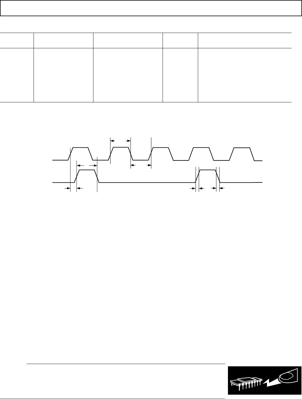
See Figure 1.
Specifications subject to change without notice.
t
3
t
2
t
1
t
4
t
HIGH
t
LOW
CLKIN
FOUT
Figure 1. Timing Diagram
TIMING CHARACTERISTICS
1, 2, 3
ABSOLUTE MAXIMUM RATINGS*
(T
A
= 25°C unless otherwise noted)
VDD to GND . . . . . . . . . . . . . . . . . . . . . . . . . –0.3 V to +7 V
Analog Input Voltage to GND . . . . . . . . –0.3 V to V
DD
+ 0.3 V
Reference Input Voltage to GND . . . . . –0.3 V to V
DD
+ 0.3 V
Logic Input Voltage to GND . . . . . . . . –0.3 V to VDD + 0.3 V
FOUT Voltage to GND . . . . . . . . . . . –0.3 V to VDD + 0.3 V
Operating Temperature Range
Commercial (K Version) . . . . . . . . . . . . . . . . 0°C to +85°C
Automotive (Y Version) . . . . . . . . . . . . . . –40°C to +105°C
Storage Temperature Range . . . . . . . . . . . . –65°C to +150°C
Junction Temperature (T
J
Max) . . . . . . . . . . . . . . . . . . 150°C
SOT-23 Package
Power Dissipation . . . . . . . . . . . . . . . . . . (T
J
Max – T
A
)/θ
JA
θ
JA
Thermal Impedance . . . . . . . . . . . . . . . . . . . . . 240°C/W
Lead Temperature (10 secs) . . . . . . . . . . . . . . . . . . 300°C
Reflow Soldering
Peak Temperature . . . . . . . . . . . . . . . . . . . . 220 + 5/0°C
Time at Peak Temperature . . . . . . . . . . . . 10 sec to 40 sec
MSOP Package
Power Dissipation . . . . . . . . . . . . . . . . . (T
J
Max – T
A
)/θ
JA
θ
JA
Thermal Impedance . . . . . . . . . . . . . . . . . . . . . 206°C/W
θ
JC
Thermal Impedance . . . . . . . . . . . . . . . . . . . . . . 44°C/W
Lead Temperature (10 secs) . . . . . . . . . . . . . . . . . . . 300°C
Reflow Soldering
Peak Temperature . . . . . . . . . . . . . . . . . . . . . . 220 +5/0°C
Time at Peak Temperature . . . . . . . . . . . . . 10 sec to 40 sec
*Stresses above those listed under Absolute Maximum Ratings may cause perma-
nent damage to the device. This is a stress rating only; functional operation of the
device at these or any other conditions above those listed in the operational
sections of this specification is not implied. Exposure to absolute maximum rating
conditions for extended periods may affect device reliability.
CAUTION
ESD (electrostatic discharge) sensitive device. Electrostatic charges as high as 4000 V readily
accumulate on the human body and test equipment and can discharge without detection. Although
the AD7740 features proprietary ESD protection circuitry, permanent damage may occur on
devices subjected to high-energy electrostatic discharges. Therefore, proper ESD precautions are
recommended to avoid performance degradation or loss of functionality.
WARNING!
ESD SENSITIVE DEVICE
–4–
PIN FUNCTION DESCRIPTIONS
8-LEAD MSOP PIN NUMBERS*
Pin
No. Mnemonic Function
1 CLKOUT The crystal/resonator is tied between this pin and CLKIN. In the case of an external clock driving CLKIN, an
inverted clock signal appears on this pin and can be used to drive other circuitry provided it is buffered first.
2 CLKIN The master clock for the device may be in the form of a crystal/resonator tied between this pin and CLKOUT.
An external CMOS-compatible clock may also be applied to this input as the clock for the device. If CLKIN
is inactive low for 1 ms (typ), the AD7740 automatically enters power-down.
3 GND Ground reference for all the circuitry on-chip.
4 REFIN/OUT Voltage Reference Input. This is the reference input to the core of the VFC and defines the span of the VFC.
If this pin is left unconnected, the internal 2.5 V reference is the default reference. Alternatively, a precision
external reference may be used to overdrive the internal reference. The internal reference has high output
impedance in order to allow it to be overdriven.
5 VIN The analog input to the VFC. It has a nominal input range from 0 V to V
REF
which corresponds to an output
frequency of 10% f
CLKIN
to 90% f
CLKIN
. It has a ±150 mV overrange. If buffered, it draws virtually no current
from whatever source is driving it.
6 VDD Power Supply Input. These parts can be operated at 3.3 V ± 10% or 5 V ± 5%. The supply should be
adequately decoupled with a 10 µF and a 0.1 µF capacitor to GND.
7 FOUT Frequency Output. FOUT goes from 10% to 90% of f
CLKIN
, depending on VIN.
8 BUF Buffered Mode Select Pin. When BUF is tied low, the VIN input is unbuffered and the range on the VIN
pin is –0.15 V to VDD + 0.15 V. When it is tied high, VIN is buffered and the range on the VIN pin
is restricted to 0.1 V to VDD – 0.2 V.
*Note that the SOT-23 and MSOP packages have different pinouts.
PIN CONFIGURATIONS
8-Lead MSOP
microSOIC
TOP VIEW
(Not to Scale)
8
7
6
5
1
2
3
4
CLKOUT
CLKIN
GND
REFIN/OUT
BUF
FOUT
VDD
VIN
AD7740
8-Lead SOT-23
SOT-23
TOP VIEW
(Not to Scale)
8
7
6
5
1
2
3
4
BUF
FOUT
VDD
VIN
CLKOUT
CLKIN
GND
REFIN/OUT
AD7740
REV. C
AD7740
ORDERING GUIDE
Model
1
Temperature Range Package Description Package Option Branding Information
8-Lead MSOP RM-8
V0K
8-Lead MSOP RM-8
V0K
8-Lead MSOP RM-8
V0K
0°C to +85°C
0°C to +85°C
0°C to +85°C
0°C to +85°C 8-Lead MSOP RM-8
V0K
8-Lead MSOP RM-8
V0Y
8-Lead MSOP RM-8
V0Y
8-Lead MSOP RM-8
V0Y
8-Lead MSOP RM-8
V0Y
AD7740KRM
AD7740KRMZ
AD7740KRMZ-REEL
AD7740KRMZ-REEL7
AD7740YRM
AD7740YRMZ
AD7740YRMZ-REEL
AD7740YRMZ-REEL7
AD7740YRTZ-REEL7
−40°C to +105°C
−40°C to +105°C
−40°C to +105°C
−40°C to +105°C
−40°C to +105°C 8-Lead SOT-23 RJ-8 C41
1
Z = RoHS Compliant Part.
AD7740
REV. C
–5–
TERMINOLOGY
INTEGRAL NONLINEARITY
For the VFC, Integral Nonlinearity (INL) is a measure of the maxi-
mum deviation from a straight line passing through the actual
endpoints of the VFC transfer function. The error is expressed in
% of the actual frequency span:
Frequency Span = FOUT(max) – FOUT(min)
OFFSET ERROR
Ideally, the output frequency for 0 V input voltage is 10% of
f
CLKIN
in unbuffered mode. The deviation from this value referred
to the input is the offset error at BUF = 0. In buffered mode the
minimum output frequency (corresponding to 0.10 V minimum
input voltage) is 13.2% of f
CLKIN
at V
REF
= 2.5 V. The deviation
from this value referred to the input is the offset error at BUF = 1.
Offset error is expressed in mV.
GAIN ERROR
This is a measure of the span error of the VFC. The gain is the
scale factor that relates the input VIN to the output FOUT.
The gain error is the deviation in slope of the actual VFC transfer
characteristic from the ideal expressed as a percentage of the full-
scale span. See Figure 2.
OFFSET ERROR DRIFT
This is a measure of the change in Offset Error with changes in
temperature. It is expressed in µV/°C.
GAIN ERROR DRIFT
This is a measure of the change in Gain Error with changes in
temperature. It is expressed in (ppm of span)/°C.
POWER SUPPLY REJECTION RATIO (PSRR)
This indicates how the apparent input voltage of the VFC is
affected by changes in the supply voltage. The input voltage is
kept constant at 2 V, V
REF
is 2.5 V and the VDD supply is varied
10% at 3.3 V and ±5% at 5 V. The ratio of the apparent change
in input voltage to the change in VDD is measured in dBs.
0
REFIN
WITH OFFSET
ERROR ONLY
IDEAL
GAIN ERROR
OUTPUT
FREQUENCY
FOUT
0.9 f
CLKIN
OFFSET
ERROR
WITH OFFSET
ERROR AND
GAIN ERROR
INPUT
VOLTAGE
VIN
0.1
f
CLKIN
Figure 2. Offset and Gain

AD7740KRMZ

Mfr. #:
Manufacturer:
Analog Devices Inc.
Description:
Voltage to Frequency & Frequency to Voltage 3/5V Low Power Sync
Lifecycle:
New from this manufacturer.
Delivery:
DHL FedEx Ups TNT EMS
Payment:
T/T Paypal Visa MoneyGram Western Union