–6–
–0.015
–0.005
0
0.005
0.01
–0.01
–0.5 0 0.5
1.51
2
2.5
VIN – V
VDD = 5V
REFIN = 2.5V
CLKIN = 1MHz
T
A
= 25C
BUFFER OFF
BUFFER ON
INL ERROR – % of Span
0.015
TPC 1. INL vs. VIN (Buffered and
Unbuffered)
VDD V
OFFSET ERROR mV
12
8
8
03 6
45
4
4
0
REFIN = 2.5V
CLKIN = 1MHz
T
A
= 25C
BUF = 0
GAIN ERROR
GAIN ERROR
OFFSET ERROR
0.08
0.04
0.12
0
0.08
0.04
GAIN ERROR % Span
TPC 4. Offset and Gain Error vs. VDD
VDD V
REFOUT V
2.520
2.500
2.5 3.0 5.5
3.5
2.515
2.510
T
A
= 25C
2.505
4.0
4.5
5.0
TPC 7. REFOUT vs. VDD
CLKIN FREQUENCY kHz
OFFSET ERROR mV
4
5
8
0 200 1000
400
6
7
600 800
V
DD
= 5V
REFIN = 2.5V
T
A
= 25C
BUFFER ON
BUFFER OFF
TPC 2. Offset Error vs. CLKIN
(Buffered and Unbuffered)
VIN V
80
1
0
5
1
23
4
PSRR dB
60
50
70
VDD = 5V
REFIN = 4.75V
CLKIN = 1MHz
T
A
= 25C
BUFFER ON
BUFFER OFF
TPC 5. PSRR vs. VIN (Buffered and
Unbuffered)
2.00V CH2 2.00V M 2.00
s
FOUT
CLKIN
2
VDD = 5V
REFIN = 5V
T
A
= 25C
CLKIN 1 MHz
1
CH1
TPC 8. Typical FOUT Pulse Train
(VIN = V
REF
/4)
CLKIN FREQUENCY kHz
0.1
0
0.05
0.05
0.1
0
200 800600400 1000
GAIN ERROR % Span
BUFFER
OFF
BUFFER ON
V
DD
= 5V
REFIN = 2.5V
T
A
= 25C
TPC 3. Gain Error vs. CLKIN
(Buffered and Unbuffered)
CLKIN FREQUENCY kHz
I
DD
mA
0
0
200
0.25
400 600 800
1000
0.5
0.75
1
1.25
BUFFER OFF
BUFFER ON
VDD = 5V
REFIN = 5V
T
A
= 25C
C
FOUT
=
43pF
C
CLKOUT
=
22pF
TPC 6. I
DD
vs. CLKIN (Buffered and
Unbuffered)
AD7740–Typical Performance Characteristics
REV. C
AD7740
REV. C
–7–
GENERAL DESCRIPTION
The AD7740 is a CMOS synchronous Voltage-to-Frequency
Converter (VFC) which uses a charge-balance conversion
technique. The input voltage signal is applied to a proprietary
front-end based around an analog modulator which converts the
input voltage into an output pulse train.
The part also contains an on-chip 2.5 V bandgap reference and
operates from a single 3.3 V or 5 V supply. A block diagram of
the AD7740 is shown in Figure 3.
VIN
INTEGRATOR
FOUT
COMPARATOR
BUF
GND
SWITCHED
CAPS
SWITCHED
CAPS
AD7740
Figure 3. Block Diagram
Input Amplifier Buffering and Voltage Range
The analog input VIN can be buffered by setting BUF = 1. This
presents a high impedance, typically 100 M, which allows
significant external source impedances to be tolerated. The VIN
voltage range is now 0.1 V to VDD – 0.2 V. By setting BUF = 0
the AD7740 input circuit accepts an analog input below GND
and the analog input VIN has a voltage range from –0.15 V to
VDD + 0.15 V. In this case the input impedance is typically
650 kΩ.
The transfer function for the AD7740 is represented by:
FOUT = 0.1 f
CLKIN
+ 0.8 (VIN/V
REF
) f
CLKIN
It is shown in Figure 4 for unbuffered mode.
V
REF
OUTPUT
FREQUENCY
FOUT
V
+ 0.15V
0.10 f
CLKIN
FOUT MIN
INPUT
VOLTAGE
VIN
FOUT MAX
0.90 f
CLKIN
0
0.15V
AD7740
Figure 4. Transfer Function
Sample Calculation:
V
REF
= 2.5 V, BUF = 0
FOUT (min) = 0.1 f
CLKIN
+ 0.8(–0.15/2.5) f
CLKIN
= 0.052 f
CLKIN
FOUT (max) = 0.1 f
CLKIN
+ 0.8(2.65/2.5) f
CLKIN
= 0.948 f
CLKIN
VFC Modulator
The analog input signal to the AD7740 is continuously sampled
by a switched capacitor modulator whose sampling rate is set
by a master clock. The input signal may be buffered on-chip
(BUF = 1) before being applied to the sampling capacitor of the
modulator. This isolates the sampling capacitor charging currents
from the analog input pin.
This system is a negative feedback loop that acts to keep the net
charge on the integrator capacitor at zero, by balancing charge
injected by the input voltage with charge injected by V
REF
. The
output of the comparator provides the digital input for the 1-bit
DAC, so that the system functions as a negative feedback loop
that acts to minimize the difference signal. See Figure 5.
INTEGRATOR
COMPARATOR
1-BIT
BITSTREAM
+V
REF
INPUT
CLK
V
REF
AD7740
Figure 5. Modulator Loop
The digital data that represents the analog input voltage is con-
tained in the duty cycle of the pulse train appearing at the output
of the comparator. The output is a pulse train whose frequency
depends on the analog input signal. A full-scale input gives an
output frequency of 0.9 f
CLKIN
and zero-scale input gives an
output frequency of 0.1 f
CLKIN
. The output allows simple inter-
facing to either standard logic families or opto-couplers. The
pulsewidth of FOUT is fixed and is determined by the high period
of CLKIN. The pulse is synchronized to the rising edge of the
clock signal. The delay time between the edge of CLKIN and the
edge of FOUT is typically 35 ns. Figure 6 shows the waveform
of this frequency output. (See TPC 8.)
3t
CLKIN
FOUT = f
CLKIN
/2
VIN = V
REF
/2
f
CLKIN
FOUT = f
CLKIN
/5
VIN = V
REF
/8
FOUT = f
CLKIN
3/10
VIN = V
REF
/4
4t
CLKIN
AVERAGE FOUT IS f
CLKIN
3/10 BUT THE ACTUAL PULSE STREAM VARIES
BETWEEN f
CLKIN
/3 and f
CLKIN
/4
Figure 6. Frequency Output Waveforms
If there is a step change in input voltage, there is a settling time
that must elapse before valid data is obtained. This is typically
two CLKIN cycles.
–8–
Clock Generation
As distinct from the asynchronous VFCs that rely on the
stability of an external capacitor to set their full-scale frequency,
the AD7740 uses an external clock to define the full-scale output
frequency. The result is a more stable transfer function, which
allows the designer to determine the system stability and drift
based upon the selected external clock.
The AD7740 requires a master clock input, which may be an
external CMOS-compatible clock signal applied to the CLKIN
pin (CLKOUT not used). For a frequency of 1 MHz, a crystal
or resonator can be connected between CLKIN and CLKOUT
so that the clock circuit functions as a crystal controlled oscilla-
tor. Figure 7 shows a simple model of this.
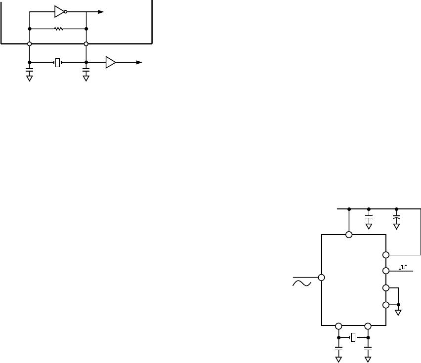
CLKIN
CLKOUT
5M
C1
C2
ON-CHIP
CIRCUITRY
OFF-CHIP
CIRCUITRY
Figure 7. On-Chip Oscillator
Using the part with a crystal or ceramic resonator between the
CLKIN and CLKOUT pins generally causes more current to
be drawn from VDD than when the part is clocked from a driven
clock signal at the CLKIN pin. This is because the on-chip
oscillator is active in the case of the crystal or resonator. The
amount of additional current depends on a number of factors.
First, the larger the value of the capacitor on CLKIN and
CLKOUT pins, the larger the current consumption. Typical
values recommended by the crystal and resonator manufacturers
are in the range of 30 pF to 50 pF. Another factor that influ-
ences I
DD
is Effective Series Resistance of the crystal (ESR).
The lower the ESR value, the lower the current taken by the
oscillator circuit.
The on-chip oscillator also has a start-up time associated with it
before it oscillates at its correct frequency and voltage levels. The
typical start-up time is 10 ms with a V
DD
of 5 V and 15 ms with
a V
DD
of 3.3 V (both with a 1 MHz crystal).
The AD7740 master clock appears inverted on the CLKOUT
pin of the device. The maximum recommended load on this pin is
one CMOS load. When using a crystal to generate the AD7740’s
clock it may be desirable to then use this clock as the clock
source for the entire system. In this case, it is recommended that
the CLKOUT signal be buffered with a CMOS buffer before
being applied to the rest of the circuit (as shown in Figure 7).
Reference Input
The AD7740 performs conversions relative to the applied refer-
ence voltage. This reference may be taken from the internal 2.5 V
bandgap reference by leaving REFIN/OUT unconnected. Alterna-
tively an external precision reference may be used. This is
connected to the REFIN/OUT pin, overdriving the internal
reference. Drive capability, initial error, noise, and drift charac-
teristics should be considered when selecting an external refer-
ence. The AD780 and REF192 are suitable choices for external
references.
The internal reference is most suited to applications where
ratiometric operation of the signal source is possible. Using the
internal reference in systems where the signal source varies with
time, temperature, loading, etc., tends to cancel out errors.
Power-Down Mode
When CLKIN is inactive low for 1 ms (typ), the AD7740 auto-
matically enters a power-down mode. In this mode most of the
digital and analog circuitry is shut down and REFOUT floats.
FOUT goes high. This reduces the power consumption to 525 µW
max (5 V) and 360 µW (3.3 V).
APPLICATIONS
The basic connection diagram for the part is shown in Figure 8.
In the connection diagram shown, the AD7740 is configured in
unbuffered mode. The 5 V power supply is used as a reference to
the AD7740. A quartz crystal provides the master clock source
for the part. It may be necessary to connect capacitors (C1 and
C2 in the diagram) to the crystal to ensure that it does not oscil-
late at overtones of its fundamental operating frequency. The
values of capacitors will vary depending on the manufacturer’s
specifications.
REFIN
AD7740
CLKIN
CLKOUT
C1 C2
FOUT
GND
BUF
0.1F
10F
VIN
VDD
5V
Figure 8. Basic Connection Diagram
AD7740
REV. C

AD7740KRMZ

Mfr. #:
Manufacturer:
Analog Devices Inc.
Description:
Voltage to Frequency & Frequency to Voltage 3/5V Low Power Sync
Lifecycle:
New from this manufacturer.
Delivery:
DHL FedEx Ups TNT EMS
Payment:
T/T Paypal Visa MoneyGram Western Union