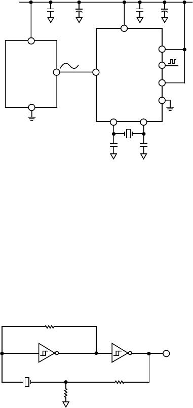
AD7740
REV. C
–9–
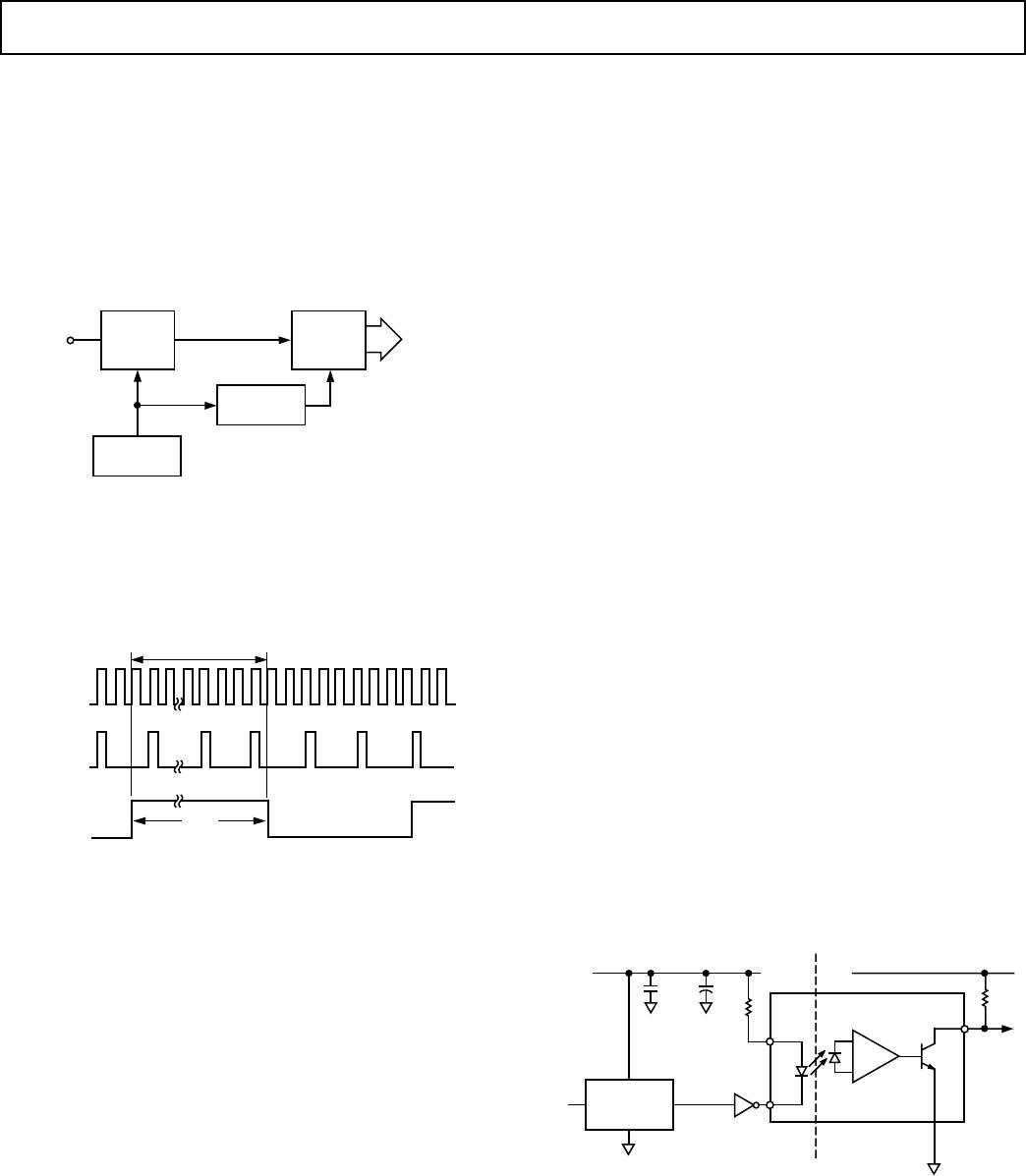
A/D Conversion Techniques Using the AD7740
One method of using a VFC in an A/D system is to count the
output pulses of FOUT for a fixed gate interval (see Figure 9).
This fixed gate interval should be generated by dividing down
the clock input frequency. This ensures that any errors due to
clock jitter or clock frequency drift are eliminated. The ratio of
the FOUT frequency to the clock frequency is what is important
here, not the absolute value of FOUT. The frequency divi-
sion can be done by a binary counter where CLKIN is the
counter input.
FREQUENCY
DIVIDER
GATE
SIGNAL
FOUT
VIN
TO P
AD7740
COUNTER
CLOCK
GENERATOR
CLKIN
Figure 9. A/D Conversion Using the AD7740 VFC
Figure 10 shows the waveforms of CLKIN, FOUT, and the
Gate signal. A counter counts the rising edges of FOUT while the
Gate signal is high. Since the gate interval is not synchronized with
FOUT, there is a possibility of a counting inaccuracy. Depending
on FOUT, an error of one count may occur.
GATE
t
GATE
FOUT
CLKIN
Figure 10. Waveforms in an A/D Converter Using a VFC
The clock frequency and the gate time determine the resolution
of such an ADC. If 12-bit resolution is required and CLKIN is
1 MHz (therefore, FOUT
MAX
is 0.9 MHz), the minimum gate
time required is calculated as follows:
N counts at Full Scale (0.9 MHz) will take
(N/0.9 × 10
6
) seconds = minimum gate time
N is the total number of codes for a given resolution; 4096 for
12 bits.
minimum gate time = (4096/0.9 × 10
6
) seconds = 4.551 ms
Since T
GATE
× FOUT
MAX
= number of counts at full scale, the
fastest conversion for a given resolution can be performed with
the highest CLKIN frequency.
If the output frequency is measured by counting pulses gated to
a signal derived from the clock, the clock stability is unimportant
and the device simply performs as a voltage-controlled frequency
divider, producing a high-resolution ADC. The inherent mono-
tonicity of the transfer function and wide range of input clock
frequencies allows the conversion time and resolution to be
optimized for specific applications.
Another parameter is taken into account when choosing the
length of the gate interval. Because the integration period of the
VFC is equal to the gate interval, any interfering signal can be
rejected by counting for an integer number of periods of the
interfering signal. For example, a gate interval of 100 ms will
give normal-mode rejection of 50 Hz and 60 Hz signals.
Isolation Applications
The AD7740 can also be used in isolated analog signal trans-
mission applications. Due to noise, safety requirements or distance,
it may be necessary to isolate the AD7740 from any controlling
circuitry. This can easily be achieved by using opto-isolators.
This is extremely useful in overcoming ground loops between
equipment.
The analog voltage to be transmitted is converted to a pulse
train using the VFC. An opto-isolator circuit is used to couple
this pulse train across an isolation barrier using light as the
connecting medium. The input LED of the isolator is driven
from the output of the AD7740. At the receiver side, the output
transistor is operated in the photo-transistor mode. The pulse
train can be reconverted to an analog voltage using a frequency-
to-voltage converter; alternatively, the pulse train can be fed into
a counter to generate a digital signal.
The analog and digital sections of the AD7740 have been designed
to allow operation from a single-ended power source, simplify-
ing its use with isolated power supplies.
Figure 11 shows a general purpose VFC circuit using a low cost
opto-isolator. A 5 V power supply is assumed for both the iso-
lated (V
DD
) and local (V
CC
) supplies.
VIN
FOUT
GND1
V
CC
GND2
ISOLATION
BARRIER
R
0.1F 10F
AD7740
V
DD
OPTOCOUPLER
Figure 11. Opto-Isolated Application
–10–
Temperature Sensor Application
The AD7740 can be used with an AD22100S temperature
sensor to give a digital measure of ambient temperature. The
output voltage of the AD22100S is proportional to the tempera-
ture times the supply voltage. It uses a single 5 V supply, and its
output swings from 0.25 V at –50°C to 4.75 V at +150°C. By
feeding its output through the AD7740, the value of ambient
temperature is converted into a digital pulse train. See Figure 12.
REFIN
AD7740
AD22100S
V+
CLKIN CLKOUT
C1 C2
FOUT
GND
BUF
0.1F
10F 0.1F
VIN
VDD
5V
10F
Figure 12. Using the AD7740 with a Temperature Sensor
Due to its ratiometric nature this application provides an
extremely cost-effective solution. The need for an external pre-
cision reference is eliminated since the 5 V power-supply is used
as a reference to both the VFC and the AD22100S.
32 kHz Operation
The AD7740 oscillator circuit will not operate at 32 kHz. If
the user wishes to use a 32 kHz watch crystal, some additional
external circuitry is required. The circuit in Figure 13 is for a
crystal with a required drive of 1 µW. Resistors R1 and R2
reduce the power to this level.
R3
1M
CLKIN
R2
100k
R1
220k
32kHz
40106
40106
Figure 13. 32 kHz Watch Crystal Circuit
Power Supply Bypassing and Grounding
In any circuit where accuracy is important, careful consideration
of the power supply and ground return layout helps to ensure
the rated performance. The printed circuit board housing the
AD7740 should be designed such that the analog and digital
sections are separated and confined to certain areas of the board.
To minimize capacitive coupling between them, digital and
analog ground planes should only be joined in one place, close
to the AD7740, and should not overlap.
Avoid running digital lines under the device, as these will couple
noise onto the die. The analog ground plane should be allowed
to run under the AD7740 to avoid noise coupling. The power
supply lines to the AD7740 should use as large a trace as pos-
sible to provide low impedance paths and reduce the effects of
glitches on the power supply line. Fast switching signals like
clocks should be shielded with digital ground to avoid radiating
noise to other parts of the board, and clock signals should never
be run near analog inputs. Avoid crossover of digital and analog
signals. Traces on opposite sides of the board should run at right
angles to each other. This reduces the effect of feedthrough
through the board. A microstrip technique is by far the best but
is not always possible with a double-sided board. In this technique,
the component side of the board is dedicated to the ground plane
while the signal traces are placed on the solder side.
Good decoupling is also important. All analog supplies should
be decoupled to GND with surface mount capacitors, 10 µF in
parallel with 0.1 µF located as close to the package as possible,
ideally right up against the device. The lead lengths on the by-
pass capacitor should be as short as possible. It is essential that
these capacitors be placed physically close to the AD7740 to
minimize the inductance of the PCB trace between the capacitor
and the supply pin. The 10 µF are the tantalum bead type and
are located in the vicinity of the VFC to reduce low-frequency
ripple. The 0.1 µF capacitors should have low Effective Series
Resistance (ESR) and Effective Series Inductance (ESI), such
as the common ceramic types, which provide a low imped-
ance path to ground at high frequencies to handle transient
currents due to internal logic switching. Additionally, it is ben-
eficial to have large capacitors (> 47 µF) located at the point
where the power connects to the PCB.
AD7740
REV. C
AD7740
REV. C
–11–
OUTLINE DIMENSIONS
8-Lead Mini Small Outline Package [MSOP]
(RM-8)
Dimensions shown in millimeters
COMPLIANT TO JEDEC STANDARDS MO-187-AA
0.80
0.55
0.40
4
8
1
5
0.65 BSC
0.40
0.25
1.10 MAX
3.20
3.00
2.80
COPLANARITY
0.10
0.23
0.09
3.20
3.00
2.80
5.15
4.90
4.65
PIN 1
IDENTIFIER
15° MAX
0.95
0.85
0.75
0.15
0.05
10-07-2009-B
COMPLIANT TO JEDEC STANDARDS MO-178-BA
8-Lead Small Outline Transistor Package [SOT-23]
(RJ-8)
Dimensions shown in millimeters
SEATING
PLANE
1.95
BSC
0.65 BSC
0.60
BSC
7 6
1 2 3 4
5
3.00
2.90
2.80
3.00
2.80
2.60
1.70
1.60
1.50
1.30
1.15
0.90
0.15 MAX
0.05 MIN
1.45 MAX
0.95 MIN
0.22 MAX
0.08 MIN
0.38 MAX
0.22 MIN
0.60
0.45
0.30
PIN 1
INDICATOR
8
12-16-2008-A

AD7740YRMZ

Mfr. #:
Manufacturer:
Analog Devices Inc.
Description:
Voltage to Frequency & Frequency to Voltage 3/5V Low Power Sync
Lifecycle:
New from this manufacturer.
Delivery:
DHL FedEx Ups TNT EMS
Payment:
T/T Paypal Visa MoneyGram Western Union