AD7740
REV. C
–3–
(VDD = 3.0 V to 3.6 V, 4.75 V to 5.25 V, GND = O V, REFIN = 2.5 V)
Limit at T
MIN
, T
MAX
Limit at T
MIN
, T
MAX
Parameter VDD = 3.0 V to 3.6 V VDD = 4.75 V to 5.25 V Unit Conditions/Comments
f
CLKIN
32 32 kHz min Clock Frequency
1 1 MHz max
t
HIGH
:t
LOW
40:60 40:60 min Clock Mark/Space Ratio
60:40 60:40 max
t
1
50 35 ns typ CLKIN Edge to FOUT Edge Delay
t
2
2.3 1.8 ns typ FOUT Rise Time
t
3
1.6 1.4 ns typ FOUT Fall Time
t
4
t
HIGH
± 20
t
HIGH
± 8
ns typ FOUT Pulsewidth
NOTES
1
Guaranteed by design and characterization, not production tested.
2
All input signals are specified with tr = tf = 5 ns (10% to 90% of VDD) and timed from a voltage level of (V
IL
+ V
IH
)/2.
3
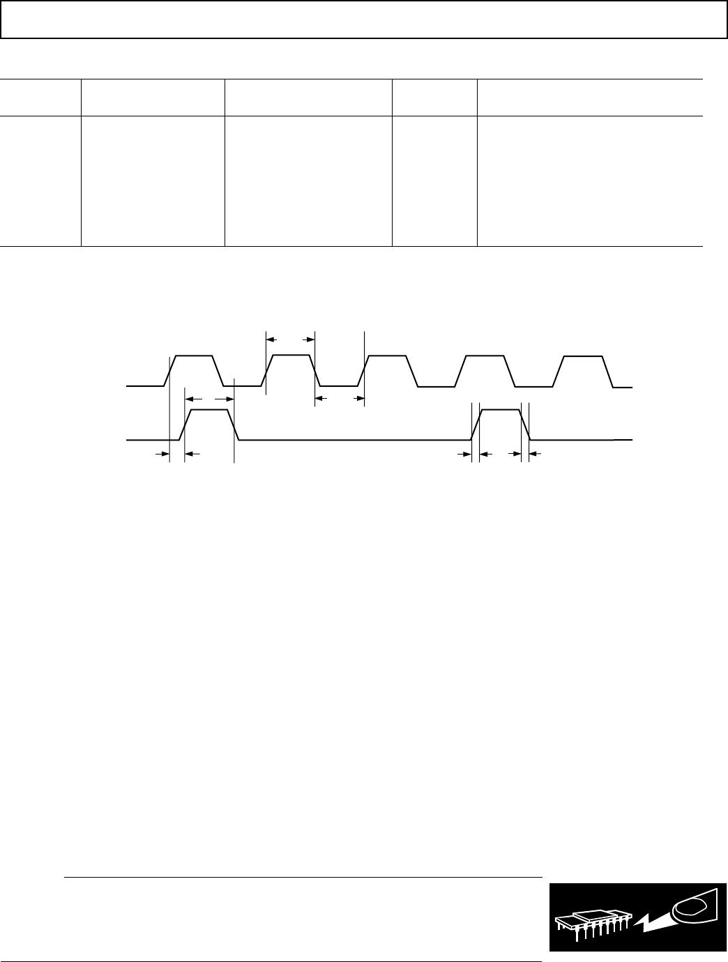
See Figure 1.
Specifications subject to change without notice.
t
3
t
2
t
1
t
4
t
HIGH
t
LOW
CLKIN
FOUT
Figure 1. Timing Diagram
TIMING CHARACTERISTICS
1, 2, 3
ABSOLUTE MAXIMUM RATINGS*
(T
A
= 25°C unless otherwise noted)
VDD to GND . . . . . . . . . . . . . . . . . . . . . . . . . –0.3 V to +7 V
Analog Input Voltage to GND . . . . . . . . –0.3 V to V
DD
+ 0.3 V
Reference Input Voltage to GND . . . . . –0.3 V to V
DD
+ 0.3 V
Logic Input Voltage to GND . . . . . . . . –0.3 V to VDD + 0.3 V
FOUT Voltage to GND . . . . . . . . . . . –0.3 V to VDD + 0.3 V
Operating Temperature Range
Commercial (K Version) . . . . . . . . . . . . . . . . 0°C to +85°C
Automotive (Y Version) . . . . . . . . . . . . . . –40°C to +105°C
Storage Temperature Range . . . . . . . . . . . . –65°C to +150°C
Junction Temperature (T
J
Max) . . . . . . . . . . . . . . . . . . 150°C
SOT-23 Package
Power Dissipation . . . . . . . . . . . . . . . . . . (T
J
Max – T
A
)/θ
JA
θ
JA
Thermal Impedance . . . . . . . . . . . . . . . . . . . . . 240°C/W
Lead Temperature (10 secs) . . . . . . . . . . . . . . . . . . 300°C
Reflow Soldering
Peak Temperature . . . . . . . . . . . . . . . . . . . . 220 + 5/0°C
Time at Peak Temperature . . . . . . . . . . . . 10 sec to 40 sec
MSOP Package
Power Dissipation . . . . . . . . . . . . . . . . . (T
J
Max – T
A
)/θ
JA
θ
JA
Thermal Impedance . . . . . . . . . . . . . . . . . . . . . 206°C/W
θ
JC
Thermal Impedance . . . . . . . . . . . . . . . . . . . . . . 44°C/W
Lead Temperature (10 secs) . . . . . . . . . . . . . . . . . . . 300°C
Reflow Soldering
Peak Temperature . . . . . . . . . . . . . . . . . . . . . . 220 +5/0°C
Time at Peak Temperature . . . . . . . . . . . . . 10 sec to 40 sec
*Stresses above those listed under Absolute Maximum Ratings may cause perma-
nent damage to the device. This is a stress rating only; functional operation of the
device at these or any other conditions above those listed in the operational
sections of this specification is not implied. Exposure to absolute maximum rating
conditions for extended periods may affect device reliability.
CAUTION
ESD (electrostatic discharge) sensitive device. Electrostatic charges as high as 4000 V readily
accumulate on the human body and test equipment and can discharge without detection. Although
the AD7740 features proprietary ESD protection circuitry, permanent damage may occur on
devices subjected to high-energy electrostatic discharges. Therefore, proper ESD precautions are
recommended to avoid performance degradation or loss of functionality.
WARNING!
ESD SENSITIVE DEVICE