IDT8N3DV85CCD REVISION A OCTOBER 30, 2013 4 ©2013 Integrated Device Technology, Inc.
IDT8N3DV85 Data Sheet LVPECL DUAL-FREQUENCY PROGRAMMABLE VCXO
Principles of Operation
The block diagram consists of the internal 3rd overtone crystal and
oscillator which provide the reference clock f
XTAL
of 114.285MHz.
The PLL includes the FemtoClock
®
VCO along with the Pre-divider
(P), the feedback divider (M) and the post divider (N). The P, M, and
N dividers determine the output frequency based on the f
XTAL
reference. The feedback divider is fractional supporting a huge
number of output frequencies. Internal registers are used to hold up
to two different factory pre-set configuration settings. The
configuration is selected via the FSEL pin. Changing the FSEL
control results in an immediate change of the output frequency to the
selected register values. The P, M, and N frequency configurations
support an output frequency range 15.476MHz to 866.67MHz and
975MHz to 1,300MHz.
The devices use the fractional feedback divider with a delta-sigma
modul
ator for noise shaping and robust frequency synthesis
capability. The relatively high reference frequency minimizes phase
noise generated by frequency multiplication and allows more efficient
shaping of noise by the delta-sigma modulator. The output frequency
is determined by the 2-bit pre-divider (P), the feedback divider (M)
and the 7-bit post divider (N). The feedback divider (M) consists of
both a 7-bit integer portion (MINT) and an 18-bit fractional portion
(MFRAC) and provides the means for high-resolution frequency
generation. The output frequency f
OUT
is calculated by:
(1)
f
OUT
f
XTAL
1
PN
------------
MINT
MFRAC 0.5+
2
18
-------------------------------------
+=
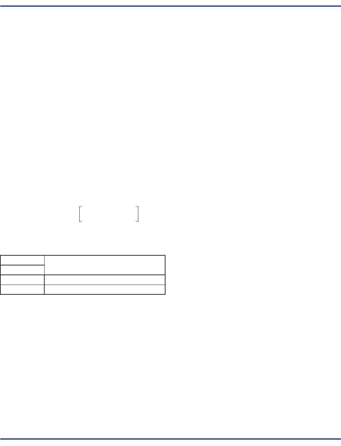
Input
SelectsFSEL
0 (default) Frequency 0
1 Frequency 1
Frequency Configuration
An order code is assigned to each frequency configuration and the
VCXO pull-range programmed by the factory (default frequencies).
For more information on the available default frequencies and order
codes, please see the Ordering Information Section in this document.
For available order codes, see the FemtoClock NG
Ceramic-Package XO and VCXO Ordering Product Information
document.
For more information on programming capabilities of the device for
custom frequ
ency and pull-range configurations, see the FemtoClock
NG Ceramic 5x7 Module Programming Guide.
Table 3A. Frequency Selection