Pin configuration LD3985
4/22 DocID9587 Rev 15
2 Pin configuration
Figure 2. Pin connections (SOT and TSOT top view, Flip-chip top view)
Flip-chip
SOT23-5L/TSOT23-5L
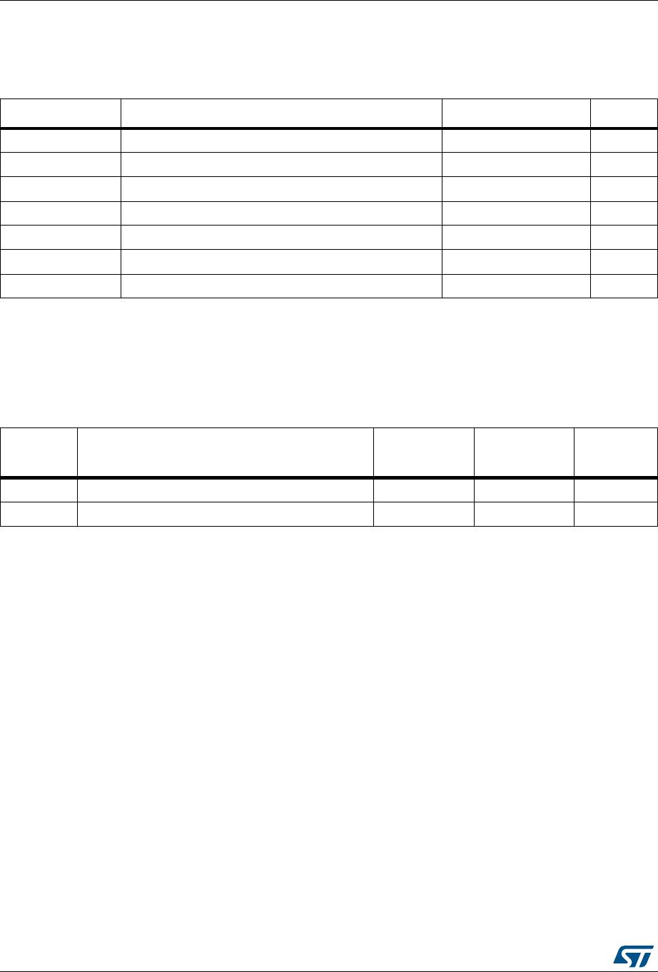
Table 2. Pin description
Pin n° for
SOT23-5L/
TSOT23-5L
Pin n° for
Flip-chip
Symbol Name and function
14V
I
Input voltage of the LDO
2 2 GND Common ground
31V
INH
Inhibit input voltage: ON mode when V
INH
1.2 V, OFF mode when V
INH
0.4 V (Do not leave it floating, not internally pulled down/up)
4 5 BYPASS
Bypass pin: an external capacitor (usually 10 nF) has to be connected to
minimize noise voltage
53V
O
Output voltage of the LDO
DocID9587 Rev 15 5/22
LD3985 Typical application
22
3 Typical application
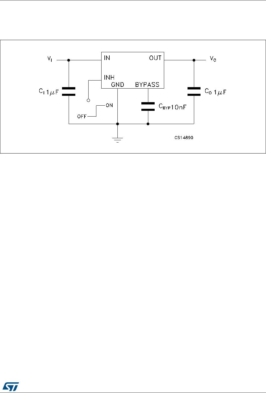
Figure 3. Typical application circuit
Maximum ratings LD3985
6/22 DocID9587 Rev 15
4 Maximum ratings
Note: Absolute maximum ratings are those values beyond which damage to the device may occur.
Functional operation under these conditions is not implied.
Table 3. Absolute maximum ratings
Symbol Parameter Value Unit
V
I
DC input voltage -0.3 to 6
(1)
1. The input pin is able to withstand non repetitive spike of 6.5 V for 200 ms.
V
V
O
DC output voltage -0.3 to V
I
+0.3 V
V
INH
Inhibit input voltage -0.3 to V
I
+0.3 V
I
O
Output current Internally limited
P
D
Power dissipation Internally limited
T
STG
Storage temperature range -65 to 150 °C
T
OP
Operating junction temperature range -40 to 125 °C
Table 4. Thermal data
Symbol Parameter
SOT23-5L/
TSOT23
Flip-chip Unit
R
thJC
Thermal resistance junction-case 81 °C/W
R
thJA
Thermal resistance junction-ambient 255 170 °C/W

LD3985M18R

Mfr. #:
Manufacturer:
STMicroelectronics
Description:
LDO Voltage Regulators 1.8V 0.15A Ultra Low
Lifecycle:
New from this manufacturer.
Delivery:
DHL FedEx Ups TNT EMS
Payment:
T/T Paypal Visa MoneyGram Western Union