DocID9587 Rev 15 7/22
LD3985 Electrical characteristics
22
5 Electrical characteristics
T
J
= 25 °C, V
I
= V
O(NOM)
+0.5 V, C
I
= 1 µF, C
BYP
= 10 nF, I
O
= 1 mA, V
INH
= 1.4 V, unless
otherwise specified.
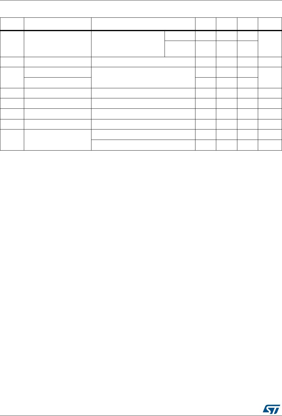
Table 5. LD3985 electrical characteristics
Symbol Parameter Test conditions Min. Typ. Max. Unit
V
I
Operating input voltage 2.5 6 V
V
O
Output voltage accuracy,
V
O(NOM)
< 2.5 V
I
O
= 1 mA -50 50
mV
T
J
= -40 to 125 °C -75 75
V
O
Output voltage accuracy,
V
O(NOM)
2.5V
I
O
= 1 mA -2 2 % of
V
O(NOM
)
T
J
= -40 to 125 °C -3 3
ΔV
O
Line regulation
(1)
V
I
= V
O(NOM)
+ 0.5 to 6 V
T
J
= -40 to 125 °C
-0.1 0.1
%/V
V
O(NOM)
= 4.7 to 5V -0.19 0.19
ΔV
O
Load regulation
I
O
= 1 mA to 150mA, V
O(NOM)
< 2.5 V
T
J
= -40 to 125 °C
0.002 0.008 %/mA
ΔV
O
Load regulation
I
O
= 1 mA to 150 mA, V
O(NOM)
2.5 V
T
J
= -40 to 125 °C (for flip-chip)
0.0004 0.002
%/mA
I
O
= 1 mA to 150mA, T
J
= -40 to 125°C
(for SOT23-5L/TSOT23-5L), V
O(NOM)
2.5 V
0.0025 0.005
ΔV
O
Output AC line regulation
(2)
V
I
= V
O(NOM)
+ 1 V, I
O
= 150 mA,
t
R
= t
F
= 30 µs
1.5 mV
PP
I
Q
Quiescent current
ON mode: V
INH
= 1.2 V
I
O
= 0 85
µA
I
O
= 0, T
J
= -40 to 125 °C 150
I
O
= 0 to 150 mA 170
I
O
= 0 to 150 mA, T
J
= -40 to 125 °C 250
OFF mode: V
INH
= 0.4 V
0.003
T
J
= -40 to 125 °C 1.5
V
DROP
Dropout voltage
(3)
I
O
= 1 mA 0.4
mV
I
O
= 1 mA, T
J
= -40 to 125 °C 2
I
O
= 50 mA 20
I
O
= 50 mA, T
J
= -40 to 125 °C 35
I
O
= 100 mA 45
I
O
= 100 mA, T
J
= -40 to 125 °C 70
I
O
= 150 mA 60
I
O
= 150 mA, T
J
= -40 to 125 °C 100
I
SC
Short-circuit current R
L
= 0 600 mA
Electrical characteristics LD3985
8/22 DocID9587 Rev 15
SVR Supply voltage rejection
V
I
= V
O(NOM)
+0.25 V ±
V
RIPPLE
= 0.1 V, I
O
= 50 mA
V
O(NOM)
< 2.5 V, V
I
= 2.55 V
f = 1kHz 60
dB
f = 10kHz 50
I
O(PK)
Peak output current V
O
V
O(NOM)
- 5% 300 550 mA
V
INH
Inhibit input logic low
V
I
= 2.5 V to 6 V, T
J
= -40 to 125 °C
0.4
V
Inhibit input logic high 1.2
I
INH
Inhibit input current V
INH
= 0.4 V, V
I
= 6 V ±1 nA
eN Output noise voltage B
W
= 10 Hz to 100 kHz, C
O
= 1 µF 30 µV
RMS
t
ON
Turn-on time
(4)
C
BYP
= 10 nF 100 250 µs
T
SHDN
Thermal shutdown
(5)
160 °C
C
O
Output capacitor
Capacitance
(6)
122µF
ESR 5 5000 mΩ
1. For V
O(NOM)
< 2 V, V
I
= 2.5 V
2. For V
O(NOM)
= 1.25 V, V
I
= 2.5 V
3. Dropout voltage is the input-to-output voltage difference at which the output voltage is 100 mV below its nominal value. This
specification does not apply to input voltages below 2.5 V
4. Turn-on time is time measured between the enable input just exceeding V
INH
high value and the output voltage just
reaching 95% of its nominal value
5. Typical thermal protection hysteresis is 20 °C
6. The minimum capacitor value is 1 µF, anyway the LD3985 is still stable if the compensation capacitor has a 30% tolerance
in all temperature range
Table 5. LD3985 electrical characteristics (continued)
Symbol Parameter Test conditions Min. Typ. Max. Unit
DocID9587 Rev 15 9/22
LD3985 Typical performance characteristics
22
6 Typical performance characteristics
T
J
= 25 °C, V
I
= V
O(NOM)
+0.5 V, C
I
= C
O
= 1 µF, C
BYP
= 10 nF, I
O
= 1 mA, V
INH
= 1.4 V,
unless otherwise specified.
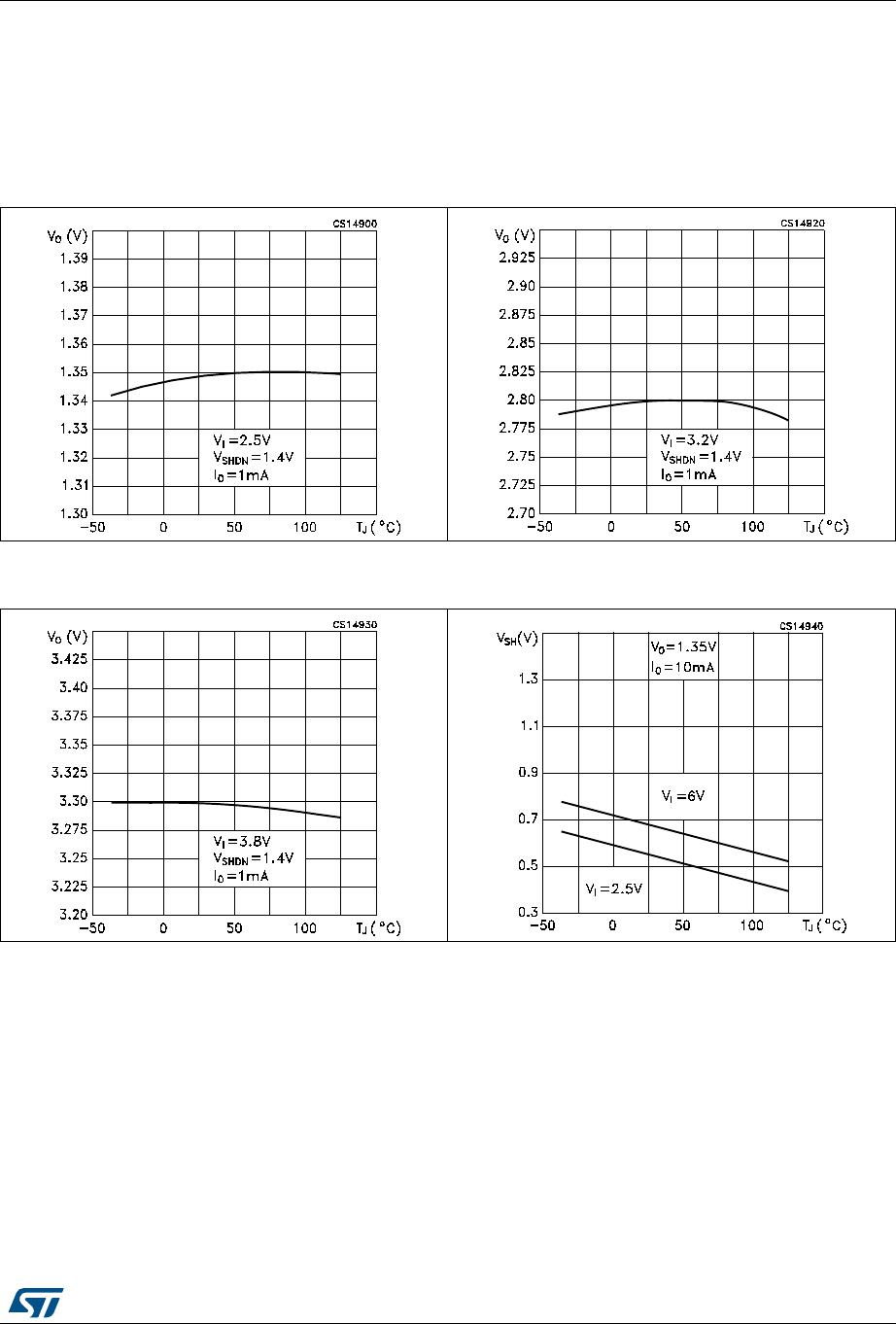
Figure 4. Output voltage vs. temperature
(V
0
=1.35 V)
Figure 5. Output voltage vs. temperature
(V
0
=2.7 V)
Figure 6. Output voltage vs. temperature
(V
0
=3.3 V)
Figure 7. Shutdown voltage vs. temperature
(V
0
=1.35 V)

LD3985M18R

Mfr. #:
Manufacturer:
STMicroelectronics
Description:
LDO Voltage Regulators 1.8V 0.15A Ultra Low
Lifecycle:
New from this manufacturer.
Delivery:
DHL FedEx Ups TNT EMS
Payment:
T/T Paypal Visa MoneyGram Western Union