Document #: 38-07291 Rev. *C Page 3 of 9
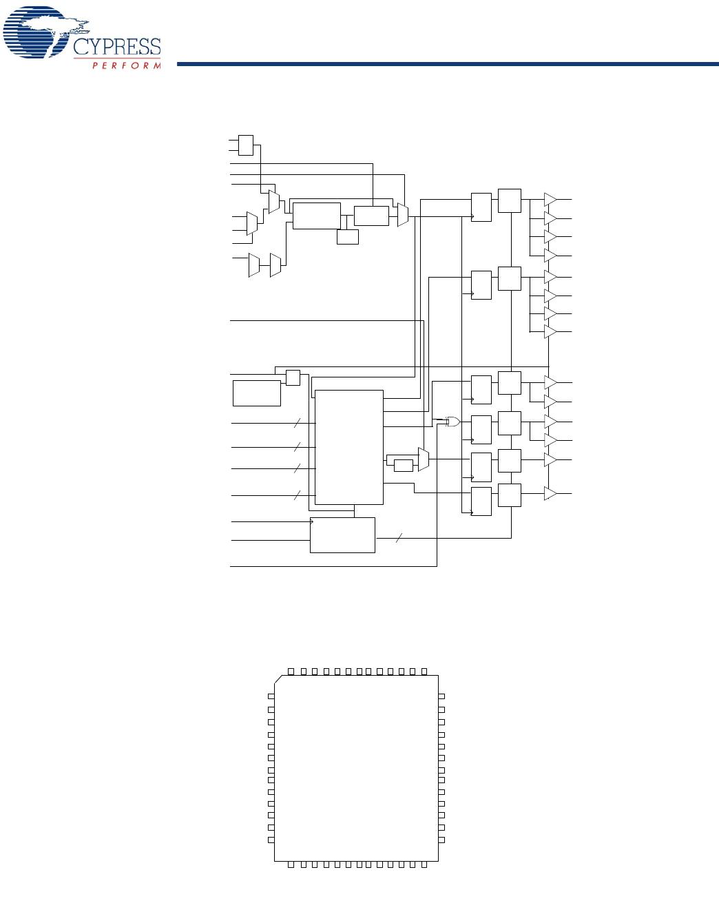
Pin Definitions
[2]
Pin Name PWR IO Type Description
11 PECL_CLK I PU PECL Clock Input.
12 PECL_CLK# I PD PECL Clock Input.
9 TCLK0 I PU External Reference or Test Clock Input.
10 TCLK1 I PU External Reference or Test Clock Input.
44, 46, 48, 50 QA(3:0) VDDC O Clock Outputs. See Table 2 on page 4 for frequency selections.
32, 34, 36, 38 QB(3:0) VDDC O Clock Outputs. See Table 2 on page 4 for frequency selections.
16, 18, 21, 23 QC(3:0) VDDC O Clock Outputs. See Table 2 on page 4 for frequency selections.
29 FB_OUT VDDC O Feedback Clock Output. Connect to FB_IN for normal operation. The
divider ratio for this output is set by FB_SEL(0:2). See Table 1 on page 1.
A bypass delay capacitor at this output control Input Reference or Output
Banks phase relationships.
25 SYNC VDDC O Synchronous Pulse Output. This output is used for system
synchronization. The rising edge of the output pulse is in sync with both
the rising edges of QA (0:3) and QC(0:3) output clocks regardless of the
divider ratios selected.
42, 43 SELA(1,0) I PU Frequency Select Inputs. These inputs select the divider ratio at QA(0:3)
outputs. See Table 2 on page 4.
40, 41 SELB(1,0) I PU Frequency Select Inputs. These inputs select the divider ratio at QB(0:3)
outputs. See Table 2 on page 4.
19, 20 SELC(1,0) I PU Frequency Select Inputs. These inputs select the divider ratio at QC(0:3)
outputs. See Table 2 on page 4.
5, 26, 27 FB_SEL(2:0) I PU Feedback Select Inputs. These inputs select the divide ratio at FB_OUT
output. See Table 1 on page 1.
52 VCO_SEL I PU VCO Divider Select Input. When set LOW, the VCO output is divided by 2.
When set HIGH, the divider is bypassed. See Table 1 on page 1.
31 FB_IN I PU Feedback Clock Input. Connect to FB_OUT for accessing the PLL.
6 PLL_EN I PU PLL Enable Input. When asserted HIGH, PLL is enabled. When LOW, PLL
is bypassed.
7 REF_SEL I PU Reference Select Input. When HIGH, the PECL inputs are selected. When
LOW, TCLK[0:1] are selected.
8 TCLK_SEL I PU TCLK Select Input. When LOW, TCLK0 is selected. When HIGH TCLK1
is selected.
2 MR#/OE I PU Master Reset or Output Enable Input. When asserted LOW, resets all of
the internal flip-flops and also disables all of the outputs. When pulled
HIGH, releases the internal flip-flops from reset and enables all of the
outputs.
14 INV_CLK I PU Inverted Clock Input. When set HIGH, QC(2,3) outputs are inverted. When
set LOW, the inverter is bypassed.
3 SCLK I PU Serial Clock Input. Clocks data at SDATA into the internal register.
4 SDATA I PU Serial Data Input. Input data is clocked to the internal register to enable or
disable individual outputs. This provides flexibility in power management.
17, 22, 28,
33,37, 45, 49
VDDC 3.3V Power Supply for Output Clock Buffers.
13 VDD 3.3V Supply for PLL.
1, 15, 24, 30,
35, 39, 47, 51
VSS Common Ground.
Note
2. A bypass capacitor (0.1μF) must be placed as close as possible to each positive power (<0.2”). If these bypass capacitors are not close to the pins their high frequency
filtering characteristics is cancelled by the lead inductance of the traces.
[+] Feedback